Functional details, Pci-dual-ac5 block diagram, Chapter 3 – Measurement Computing PCI-DUAL-AC5 User Manual
Page 13
Advertising
13
Chapter 3
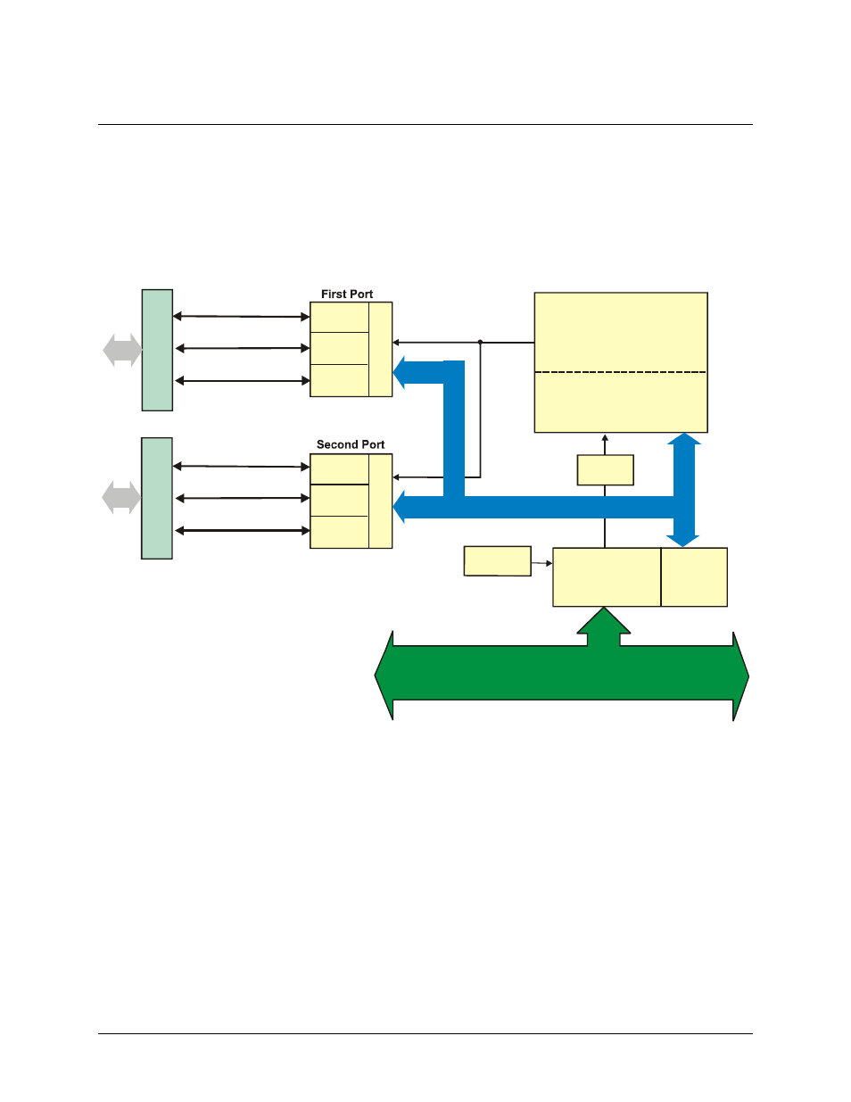
Functional Details
PCI-DUAL-AC5 block diagram
PCI-DUAL-AC5 functions are illustrated in the block diagram shown here.
PCI
Controller
BADR2
Boot
EEPROM
Control
Registers
Decode/Status
Bus
Timing
Controller FPGA and Logic
Local Bus
PCI Bus (5V, 32-bit, 33 MHZ)
Control Bus
Port A
Port B
C
o
n
tr
o
l
Port C
Port A
Port B
C
o
n
tr
o
l
FIRSTPORTA(7:0)
Port C
S
S
R
-P
B
2
4
S
S
R
-P
B
2
4
AC/DC
AC/DC
I/O Module
Racks
SECONDPORTA(7:0)
FIRSTPORTB(7:0)
FIRSTPORTB(7:0)
SECONDPORTB(7:0)
SECONDPORTC(7:0)
Figure 2. Functional block diagram
Advertising