Chapter 3, Board layout – Lanner LVC-5550S User Manual
Page 16
16
Board Layout
Chapter 3
Embedded and Industrial Computing
Pin No.
Function
Pin No.
Function
1
GND
26
CF_CD1#
2
CF_DD3
27
CF_DD11
3
CF_DD4
28
CF_DD12
4
CF_DD5
29
CF_DD13
5
CF_DD6
30
CF_DD14
6
CF_DD7
31
CF_DD15
7
CF_DCS0#
32
CF_DCS1#
8
A10(GND)
33
VS1#
9
OE#(GND)
34
CF_DIOR#
10
A9(GND) [CF_SATA_RXP]
35
CF_DIOW#
11
A8(GND) [CF_SATA_RXN]
36
WE#(VCC3)
12
A7(GND)
37
CF_IRQ#
13
VCC
38
VCC
14
A6(GND)
39
CSEL#(GND)
14
A5(GND) [CF_SATA_TXN]
39
VS2#
15
A4(GND) [CF_SATA_TXP]
40
CF_RESET#
16
A3(GND)
41
CF_IORDY
17
CF_A2
42
CF_DMARQ
18
CF_A1
43
CF_DDACK#
19
CF_A0
44
CF_ACT#
20
CF_DD0
45
CF_DIAG
21
CF_DD1
46
CF_DD8
22
CF_DD2
47
CF_DD9
23
WP(NC)
48
CF_DD10
24
CF_CD2#
49
GND
25
CD2#
50
GND
Dual USB Port Connector 0 and 1 (USB1, USB2)
Line-Out and MIC-In Connector (AUDIO1):
PS/2 Keyboard & Mouse Connector (KM1):
DC_IN CONNECTOR (DC_IN1): A Phoenix connector for
external power supply with ignition.
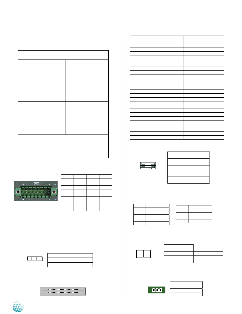
Digital IN/OUT(DGIOC1) Connector: The 12 pins of
General Purpose Input/Output (GPIO) support input and
output operations through the terminal block.
Maximum input/output current for each port is
100mA
Input/output
pins:
DI_0/DI_1/
DI_2/DI_3
DO_0/DO_1/
DO_2/DO_3
Voltage
Logic
Register
Di: <0.8V
Do: <0.4V
Low
0
DI: 10 ~ 12V
Do:12V
High
1
DI_4/DI_5
(only low
status can be
detected for
MCU control)
<0.8V
Low
0
3.3V
High
1
The default BIOS value:
0 for DI_0~DI_3, 1 for DI_4~DI_5, and 1 for DO.
Pin15 (Relay_NOPEN) and pin16 (Relay_COMM) On/
Off can be used for control of MCU DO_1: out 1(high)=
on; out 0(low)=off.
Clear CMOS jumper (CCMOS1): It is for clearing the
CMOS memory.
CompactFlash Connector (CF1): It is for connecting a
Compact Flash card to be served as your system’s storage.
Pin No.
Function
1-2
Normal (Default)
2-3
Clear CMOS
1 2 3
25 1
50 26
Pin No.
Function
1
USB power1_+5V
2
USB1_DAT-
3
USB1_DAT+
4
Ground
5
USB power0_+5V
6
USB0_DAT-
7
USB0_DAT+
8
Ground
Pin No.
Function
1
GND_AUD
2
MIC_IN_L
3
GND_AUD
4
GND_AUD
`5
MIC_IN_R
Pin No.
Pin Name
1
Ignition in
2
GND
3
9V~30V DC IN
3 2 1
1 2 3 4
5 6 7 8
Pin No. Pin Name
1
KBCLK
3
KEY
5
KEY
7
MSCLK
Pin No. Pin Name
2
GND
4
KBDAT
6
MSDATA
8
+5V
2 4 6 8
1 3 5 7
Pin No.
Pin Name
Pin No.
Pin Name
1
DI_0
2
DO_0
3
DI_1
4
DO_1
5
DI_2
6
DO_2
7
DI_3
8
DO_3
9
DI_4
10
NC
11
DI_5
12
NC
13
GND
14
GND
15
Relay_
NOPEN
16
Relay_
COMM
MIC-in Pink Jack
Line-out Lime Jack
Pin No.
Function
1
LINE_OUT_L
2
GND_AUD
3
GND_AUD
4
LINE_OUT_ R