Chapter 3, Motherboard information – Lanner FW-8759 User Manual
Page 21
15
Motherboard Information
Network Application Platforms
Chapter 3
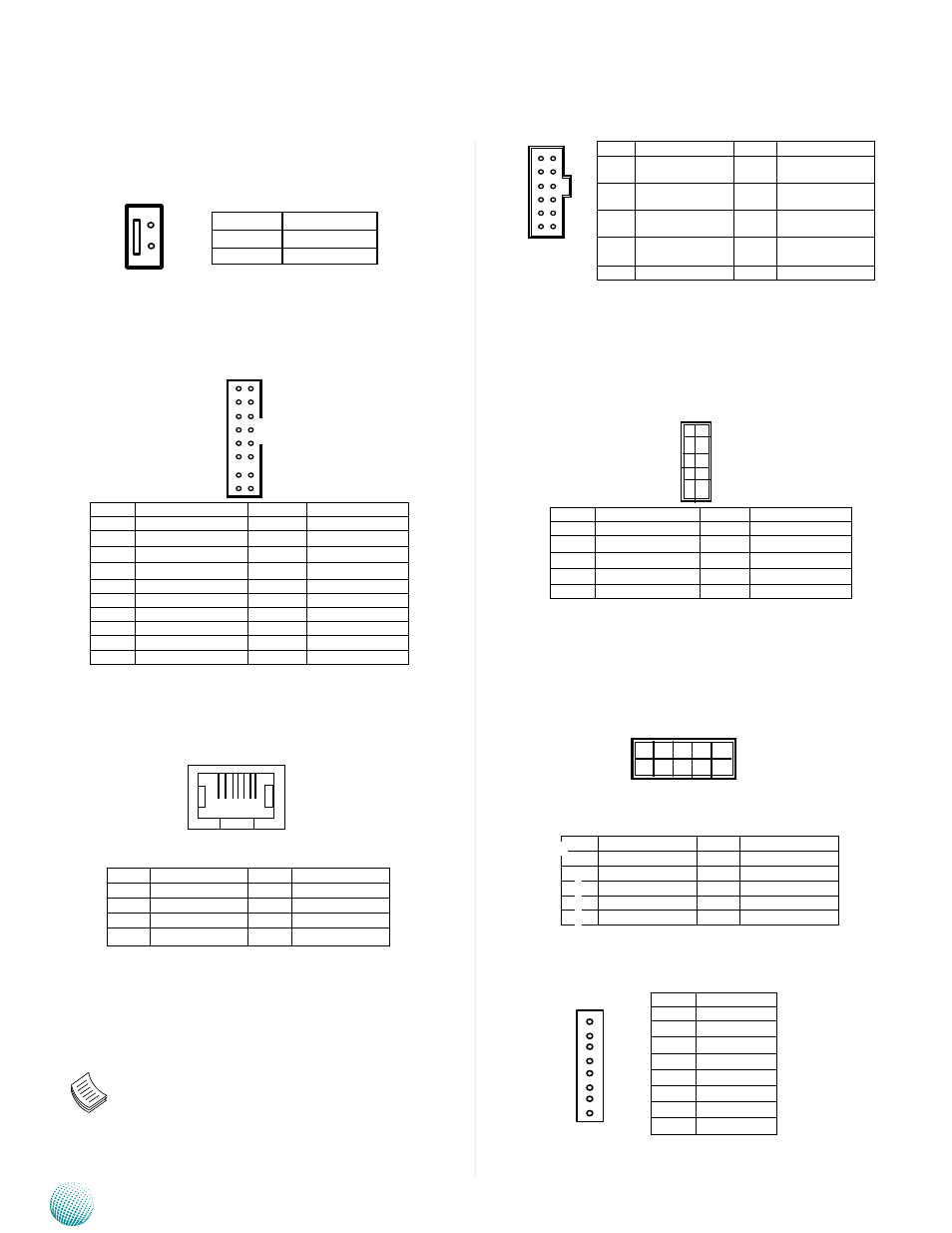
CONN1: Power-switch Connector
USB Connector USB2&USB3 (J5): It is for connecting
the USB module cable. It complies with USB3.0 .
RJ45 Console Connector (COMB2): It is for serial
communication.
Serial Interface Connectors (COMB1): It is for
connecting the RS-232 serial port interface cable.This
serial port setting can be altered in the BIOS menu:
go to BIOS->Advanced->Super IO Configuration-
>Serial Port 0 Configuration
Note: In the Super IO Configuration of the BIOS
menu, Serial Port 0 refers to the console port on
the front panel whereas Serial Port 1 refers to the
COMB1 here.
Port 80h POST Debug (80Port1): It is a proprietary
connector for connecting a checkpoint device to
generate diagnostic progess codes (POST codes)
to I/O port 80h throughput booting and Power-On
Self Test (POST) to indicate the task the system is
currently executing.
SPI-ROM Update Connector (SPIROM1): Using the
appropriate cable to connect this 10-pin ISP-in header
connector, the user can update the SPI Flash soldered
on board.
PSU PMBUS and TTL Function Connectors (CON3)
:
Pin No.
Signals
1
PWR_BTIN_N
2
GND
2
4
6
8
10
1
3
5
7
9
Pin No.
Function
Pin No.
Function
1
CLK
2
LAD1
3
RST-
4
LAD0
5
LFRAME-
6
P3V3
7
LAD3
8
KEY
9
LAD2
10
GND
Pin No.
Function
Pin No.
Function
1
NC
2
USB+5
3
USB+4
4
USB-5
5
USB-4
6
GND
7
GND
8
USB3T+2
9
USB3T+1
10
USB3T-2
11
USB3T-1
12
GND
13
GND
14
USB3R+2
15
USB3R+1
16
USB3R-2
17
USB3R-1
18
V5USB2
19
V5USB2
20
NC
2
1
19
1
20
2
Pin No.
Function
Pin NO.
Function
1
Data Carrier De-
tect (DCDA#)
2
Data Set Ready
(DSRA#)
3
Receive Data
(RXDA)
4
Request To Send
(RTSA#)
5
Transmit Data
(TXDA)
6
Clear To Send
(CTSA#)
7
Data Terminal
Ready (DTRA #)
8
Ring Indicator
(RIA#)
9
Ground (GND)
10
Key
Pin No.
Function
Pin NO.
Function
1
NC
2
NC
3
SPI_CS0-
4
P3V3ME
5
SPI_MISO
6
HPLD-
7
NC
8
SPI_CLK
9
GND
10
SPI_MOSI
2
12
1
11
1 8
Pin No.
Signal
Pin NO.
Signal
1
LNRTSB#
2
LNDTRB#
3
LNSOUTB#
4
GND
5
GND
6
LNSINB
7
LNDSRB#
8
LNCTSB#
9
10
1
2
1
2
8
Pin No.
Signal
1
PSU_TTL1
2
PSU_TTL2
3
NC
4
GND
5
NC
6
PMBUS_CLK
7
PMBUS_DAT
8
GND