Chapter 3, Board layout – Lanner LEC-7070 User Manual
Page 15
15
Board Layout
Chapter 3
Embedded and Industrial Computing
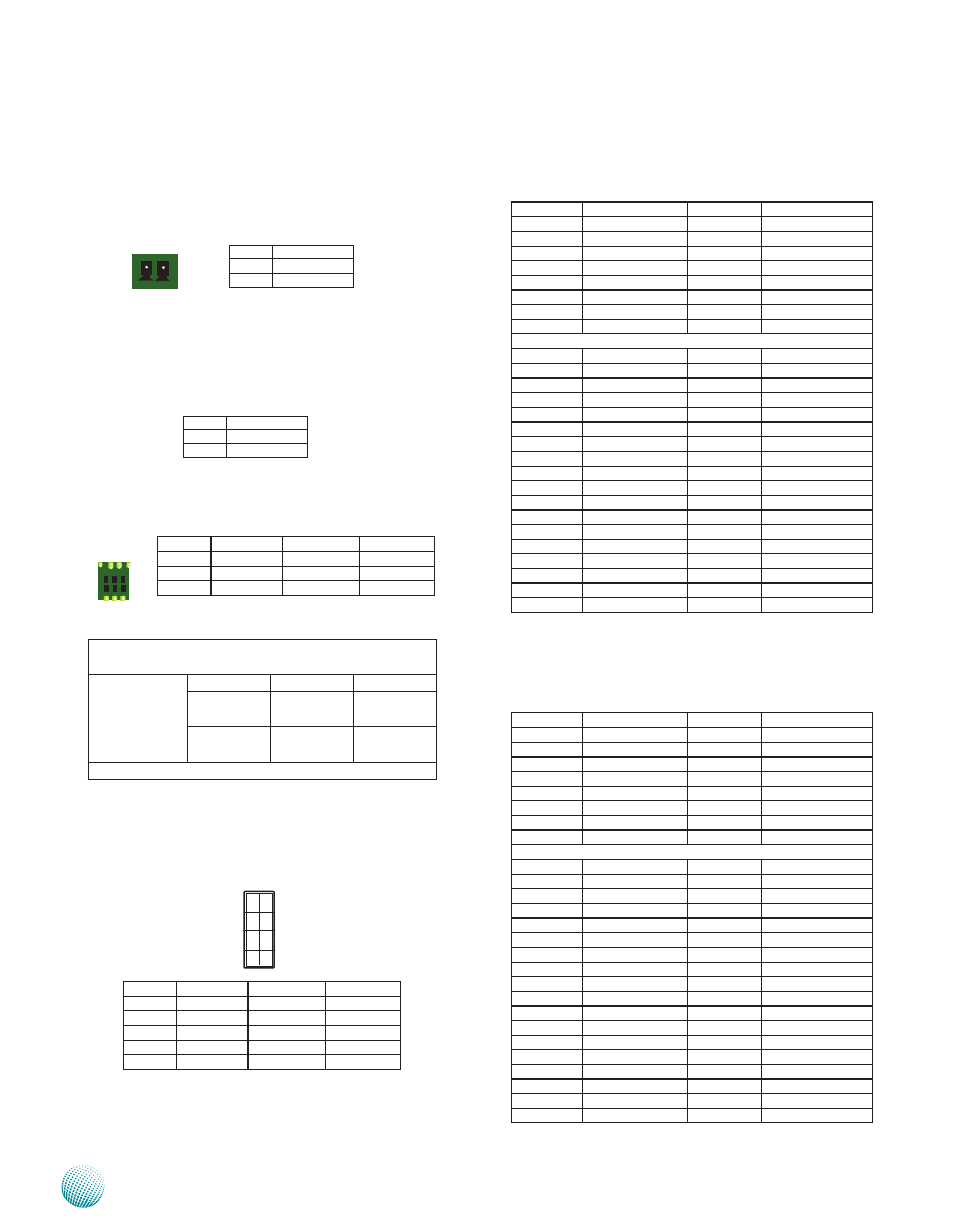
Power-on Switch through Phoenix Contact (PSBTN2): A
Phoenix connector for distant power switch.
DC_IN Power Jack (DC_IN1): A DC jack connector with
lock for external power supply.
Digital Input/Output Connector (DIO1)
Pin NO. description
Pin NO.
description
1
dIO_0
2
dIO_1
3
dIO_2
4
dIO_3
5
+5V
6
GNd
TTL Level is +5V; Maximum input/output current for
each port is 25mA
For all Input/
output pins:
Voltage
Logic
Register
DI: < 0.8V
Do: <0.4V
Low
0
DI: 2~5V
Do: 5V
High
1
The default value is 0
PS/2 Keyboard and Mouse Connector (KB1)
Pin NO. description
Pin NO.
description
1
VCC
2
MsCLK
3
MsdATA
4
KEY
5
KBdATA
6
KEY
7
GNd
8
KBCLK
Mini PCI Express Connector (for 3G card with PCI
Express 1X and USB 2.0 signals and a SIM card reader,
MPCIE1):
PIN
Pin Name
PIN
Pin Name
1
WAKE#
2
+3.3V
3
RsVd
4
GNd
5
RsVd
6
+1.5V
7
CLKREQ#
8
UIM_PWR
9
GNd
10
UIM_dATA
11
REFCLK-
12
UIM_CLK
13
REFCLK+
14
UIM_REsET
15
GNd
16
UIM_VPP
Key
17
RsVd
18
GNd
19
RsVd
20
W_dIsABLE#
21
GNd
22
PERsT#
23
PERn0
24
+3.3V
25
PERp0
26
GNd
27
GNd
28
+1.5V
29
GNd
30
sMB_CLK
31
PETn0
32
sMB_dATA
33
PETp0
34
GNd
35
GNd
36
UsB_d+
37
GNd
38
UsB_d-
39
+3.3V
40
GNd
41
+3.3V
42
LEd_WWAN#
43
GNd
44
LEd_WLAN#
45
RsVd
46
LEd_WPAN#
47
RsVd
48
+1.5V
49
RsVd
50
GNd
51
RsVd
52
+3.3V
Mini PCI Express Connector in half length (for Wi-Fi
connection with PCI Express 1X and USB 2.0 signals,
MPCIE2):
PIN
Pin Name
PIN
Pin Name
1
WAKE#
2
+3.3V
3
RsVd
4
GNd
5
RsVd
6
+1.5V
7
CLKREQ#
8
RsVd
9
GNd
10
RsVd
11
REFCLK-
12
RsVd
13
REFCLK+
14
RsVd
15
GNd
16
RsVd
Key
17
RsVd
18
GNd
19
RsVd
20
W_dIsABLE#
21
GNd
22
PERsT#
23
PERn0
24
+3.3V
25
PERp0
26
GNd
27
GNd
28
+1.5V
29
GNd
30
sMB_CLK
31
PETn0
32
sMB_dATA
33
PETp0
34
GNd
35
GNd
36
UsB_d+
37
GNd
38
UsB_d-
39
+3.3V
40
GNd
41
+3.3V
42
LEd_WWAN#
43
GNd
44
LEd_WLAN#
45
RsVd
46
LEd_WPAN#
47
RsVd
48
+1.5V
49
RsVd
50
GNd
51
RsVd
52
+3.3V
Pin No.
Pin Name
1
Ps_ON
2
GNd
2 1
Pin No.
Pin Name
1
dC_IN (+)
2
dC_IN (-)
5 1
6 2
7
5
3
1
8
6
4
2