Pin assignments, Pin # name description, Pin descriptions module description – Linx Technologies RXD-xxx-KH2 User Manual
Page 3: Theory of operation, Rf stage decoder stage
Page 5
Page 4
PIN ASSIGNMENTS
NC
D0
D1
NC
RSSI
A9
A8
A7
A6
D2
GND
VCC
PDN
D3
ANT
GND
1
2
3
4
5
6
7
8
21
22
23
24
25
26
27
28
D4
DATA
VT
A3
A2
A1
A0
D5
D6
D7
A5
A4
9
10
11
12
13
14
15
16
17
18
19
20
Figure 7: KH2 Series Receiver Pinout (Top View)
Pin #
Name
Description
1
NC
No Connection. For physical support only.
2, 3, 7, 8,
9, 12, 13,
14
D0-D7
Data Output Lines. Upon a valid transmission, these lines
will be set to replicate the state of the transmitter’s data
lines.
4
GND
Analog Ground
5
V
CC
Supply Voltage
6
PDN
Power Down. Pulling this line low will place the receiver into
a low-current state. The module will not be able to receive a
signal in this state.
10
DATA
Data output of the receiver prior to the encoder.
11
VT
Valid Transmission. This line will go high when a valid
transmission is received.
15-24
A0-A9
Address Lines. The state of these lines must match the
state of the transmitter’s address lines in order for a
transmission to be accepted.
25
RSSI
Received Signal Strength Indicator. This line will supply an
analog voltage that is proportional to the strength of the
received signal.
26
NC
No Connection. For physical support only.
27
GND
Analog Ground
28
RF IN
50-ohm RF Input
PIN DESCRIPTIONS
MODULE DESCRIPTION
The KH2 Series module combines the popular Linx LR Series receiver with a
decoder IC in a convenient SMD package. The module is ideal for general-
purpose remote control and command applications. When paired with a
matching Linx KH2 Series transmitter / encoder, OEM transmitter, LC, or LR
Series transmitter and Holtek HT640 encoder combination, a highly reliable RF
link is formed, capable of transferring control and command data over line-of-
sight distances in excess of 3,000 feet. The on-board receiver / decoder
combination provides eight switched outputs that correspond to the state of the
data lines on the transmitter’s encoder. Ten tri-state address lines are also
provided to allow up to 59,049 (3
10
) unique identification codes.
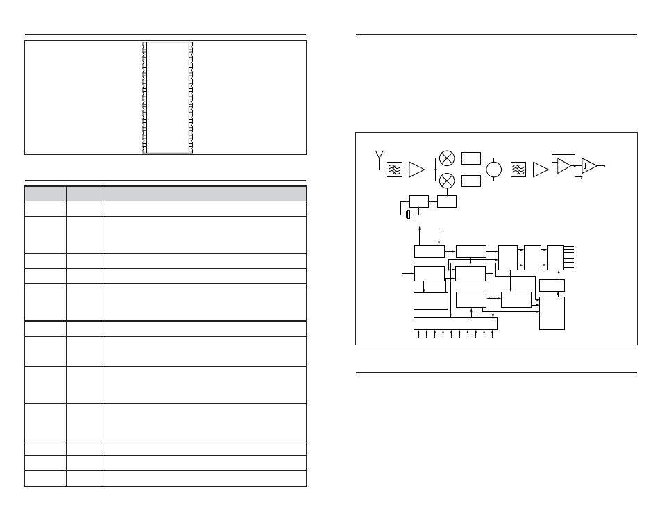
THEORY OF OPERATION
The KH2 Series receiver module is designed to receive transmissions from a
matching KH2 Series transmitter module or other compatible Linx transmitter
product. When transmitted data is received, the data is presented to the on-
board decoder. If the incoming address matches the local address settings, the
decoder’s outputs are set to replicate the states of the transmitter’s data lines.
The RF section of the KH2 module utilizes an advanced single-conversion
superhet design with a synthesized architecture, high IF frequency, and multi-
layer ceramic filters. The exceptional accuracy of the crystal-based synthesized
archetecture in the KH2 receiver module allows the receiver’s pass band to be
quite narrow, thus increasing sensitivity and reducing susceptibility to near-band
interference.
Oscillator
Buffer
Sync.
Detector
Comparator
Comparator
Data
Collector
Divider
8-bit
Shift
Register
D0
D1
D2
D3
D4
D5
D7
D6
Latch
Circuit
AND
Circuit
Buffer
Control
Logic
Transmission Gate Circuit
A0 A1 A2 A3 A4 A5 A6 A7 A8 A9
RF Stage
Decoder Stage
Data Slicer
LNA
VCO
PLL
XTAL
0˚
90˚
Limiter
Data Out
RSSI/Analog
∑
10.7MHz
IF Filter
Band Select
Filter
50
Ω RF IN
(Antenna)
+
-
Figure 8: KH2 Series Receiver Block Diagram