Theory of operation, Cts output, Power-up sequence – Linx Technologies TXM-900-HP3-xxx User Manual
Page 4: Power supply, Using the pdn pin
THEORY OF OPERATION
The HP3 Series transmitter is a high-performance, multi-channel RF transmitter
capable of transmitting both analog (FM) and digital (FSK) information. FM / FSK
modulation offers significant advantages over AM or OOK modulation methods,
including increased noise immunity and the receiver’s ability to capture in the
presence of multiple signals. This is especially helpful in crowded bands, such
as the one in which the HP3 operates.
A precision 12.00MHz Voltage Controlled Crystal Oscillator (VCXO) serves as
the frequency reference for the transmitter. Incoming data is filtered to limit the
bandwidth, and then used to directly modulate the reference. Direct reference
modulation inside the loop bandwidth provides fast start-up, while allowing a
wide modulation bandwidth and near DC modulation capability. This also
eliminates the need for code balancing.
The modulated 12.00MHz reference frequency is applied to the Phase-Locked
Loop (PLL). The PLL, combined with a 902 to 928MHz VCXO, forms a frequency
synthesizer that can be programmed to oscillate at the desired transmit
frequency. An on-board microcontroller manages the PLL programming and
greatly simplifies user interface. The microcontroller reads the channel selection
lines and programs the on-board synthesizer. This frees the designer from
complex programming requirements and allows for manual or software channel
selection. The microcontroller also monitors the status of the PLL and indicates
when the transmitter is ready to transmit data by pulling the CTS line high.
The PLL-locked carrier is amplified to increase the output power of the
transmitter and to isolate the VCO from the antenna. The output of the buffer
amplifier is connected to a filter network, which suppresses harmonic emissions.
Finally, the signal reaches the single-ended antenna port, which is matched to
50 ohms to support commonly available antennas, such as those from Linx.
CTS OUTPUT
The Clear-To-Send (CTS) output goes high to indicate that the transmitter PLL
is locked and the module is ready to accept data. In a typical application, a
microcontroller will raise the PDN line high and begin to monitor the CTS line.
When the line goes high, the microcontroller will start sending data. It is not
necessary to use the CTS output, but if not used, the circuit should wait a
minimum of 10mS after raising the PDN line high before transmitting data. If data
is being sent redundantly, there is generally no need to monitor the CTS line or
to wait a fixed time, though the initial bits may not get through.
Page 7
Page 6
Amplifier
VCO
RF OUT
Band Pass
Filter
28kHz Low Pass
Filter
DATA
IN
PLL
μP
4MHz
Int. Osc.
MODE
CS0
CS1
CS2
12MHz
Crystal
Modulator
Figure 9: HP-3 Series Transmitter Block Diagram
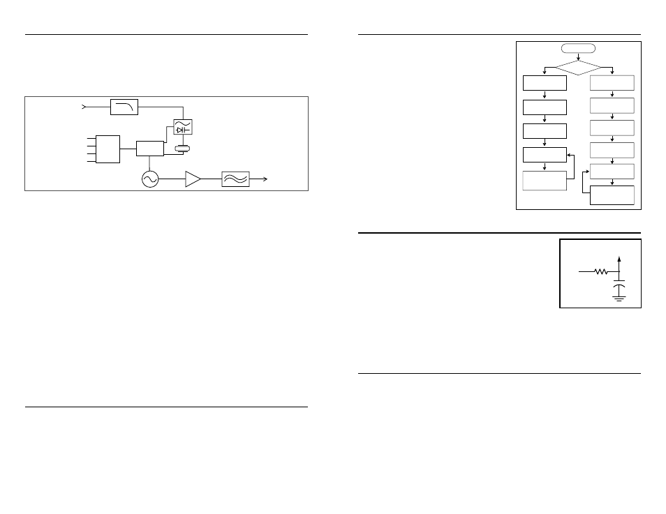
POWER-UP SEQUENCE
The HP3 transmitter is controlled by an
on-board microprocessor. When power is
applied, a start-up sequence is initiated.
At the end of the start-up sequence, the
transmitter is ready to transmit data.
The adjacent figure shows the start-up
sequence. It is executed when power is
applied to the V
CC
line or when the PDN
line is taken high.
On power-up, the micro processor reads
the external channel-selection lines and
sets the frequency synthesizer to the
appropriate channel. When the frequency
synthesizer has locked on to the proper
channel frequency, the circuit is ready to
accept data. This is acknowledged by the
CTS line transitioning high. The module
will then transmit data from the user’s
circuit.
POWER SUPPLY
The HP3 incorporates a precision, low-dropout
regulator on-board, which allows operation over an
input voltage range of 2.8 to 13 volts DC. Despite this
regulator, it is still important to provide a supply that is
free of noise. Power supply noise can significantly
affect the transmitter modulation; therefore, providing
a clean power supply for the module should be a high
priority during design.
A 10
Ω resistor in series with the supply followed by a
10µF tantalum capacitor from V
CC
to ground will help in cases where the quality
of supply power is poor. This filter should be placed close to the module’s supply
lines. These values may need to be adjusted depending on the noise present on
the supply line.
USING THE PDN PIN
The Power Down (PDN) line can be used to power down the transmitter without
the need for an external switch. This line has an internal pull-up, so when it is
held high or simply left floating, the module will be active.
When the PDN line is pulled to ground, the transmitter will enter into a low-
current (<15µA) power-down mode. During this time, the transmitter is off and
cannot perform any function.
The PDN line allows easy control of the transmitter state from external
components, such as a microcontroller. By periodically activating the transmitter,
sending data, then powering down, the transmitter’s average current
consumption can be greatly reduced, saving power in battery-operated
applications.
POWER ON
Determine Mode
Read Channel-
Selection Inputs
Program Freq. Synth
To Default CH. 50
Program Frequency
Synthesizer
Crystal Oscillator
Begins to Operate
Crystal Oscillator
Begins to Operate
Ready for
Serial Data Input
Program Frequency
Synthesizer
Determine State of
CTS Output Line
Cycle Here Until More
Data Input, Mode Change,
or PLL Loses Lock
Determine State of
CTS Output Line
Cycle Here Until
Channel
or Mode Change
Serial Mode
Parallel Mode
Figure 10: Start-up Sequence
+
10
Ω
10
μF
Vcc IN
Vcc TO
MODULE
Figure 11: Supply Filter