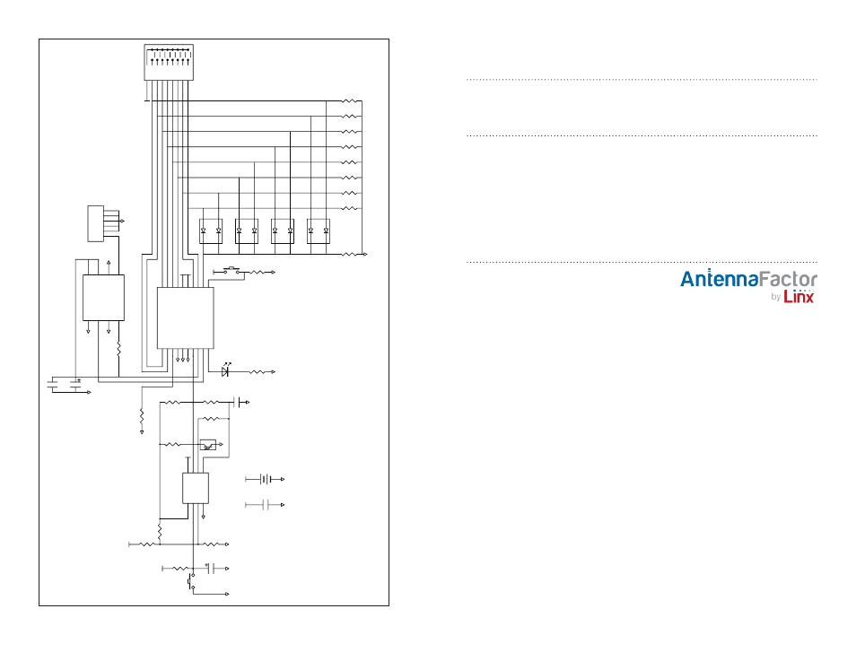
Resources, Figure 13: otx-***-hh-cp8-hs schematic diagram – Linx Technologies OTX-xxx-HH-CP8-HS User Manual
Page 10
– –
– –
14
15
Resources
Support
For technical support, product documentation, application notes, regulatory
guidelines and software updates, visit www.linxtechnologies.com
RF Design Services
For customers who need help implementing Linx modules, Linx offers
design services including board layout assistance, programming,
certification advice and packaging design. For more complex RF solutions,
Apex Wireless, a division of Linx Technologies, creates optimized designs
with RF components and firmware selected for the customer’s application.
Call +1 800 736 6677 (+1 541 471 6256 if outside the United States) for
more information.
Antenna Factor Antennas
Linx’s Antenna Factor division has the
industry’s broadest selection of antennas
for a wide variety of applications. For
customers with specialized needs, custom
antennas and design services are available along with simulations of
antenna performance to speed development. Learn more at
www.linxtechnologies.com.
VCC
R1
100k
SW1
1
SW2
2
SW3
3
SW4
4
SW5
5
SW6
6
SW7
7
SW8
8
COM
9
SM1
R2
100k
VCC
1
23
4
U3
DPAK-X2
GND
1
23
4
U5
DPAK-X2
1
23
4
U4
DPAK-X2
VCC
VCC
GND
GND
GND
S1
GND
D1
LE
D
R3
200
GND
R4
100k
GND
R5
100k
R6
100k
R7
100k
R8
100k
R9
100k
R1
0
100k
R1
1
100k
1
23
4
U2
DPAK-X2
GND
1
DATA IN
2
GND
3
LADJ/VCC
4
RF OUT
5
GND
6
VCC
7
PDN
8
TX
1
TXM-***-LR
GND
GND
GND
R1
3
D6
D7
SEL_BAUD
SEL_TIMER
GND
GND
KEY_IN
TX_CNTL
DATA_OUT
MODE_IND
CREATE_PI
N
SEND
D0
D1
VCC
VCC
D2
D3
D4
D5
U1
LICAL-ENC-HS
C3
4.7uF
C2
10pF
RFIN
1
GND
2
GND
3
GND
4
GND
5
GND
6
ANT1
SPLATCH ANTENNA
GND
Set For FCC
Compliance
VCC
GND
VCC
GND
B1
BAT-LINX2032
C1
4.7uF
GND
AOUT
1
AIN-
2
AIN+
3
GND
4
CIN+
5
CIN-
6
COUT
7
VCC
8
U6
TLV2302
R2
1
100k
VCC
R1
8
9.1M
R2
0
51k
C5
0.01uF
VCC
VCC
GND
GND
GND
GND
C4
4.7uF
R1
6
9.1M
R1
5
9.1M
R1
9
10k
R1
4
5.1M
R1
7
9.1M
IR
1
PS1102
S2
GND
GND
R2
2
100k
Figure 13: OTX-***-HH-CP8-HS Schematic Diagram