Table 3.3 chip interface control pins, Chip interface control pins, Table 3.3 – Avago Technologies LSI53C140 User Manual
Page 43
Advertising
General Description
3-9
Ver. 2.1
Copyright © 1998–2001 by LSI Logic Corporation. All rights reserved.
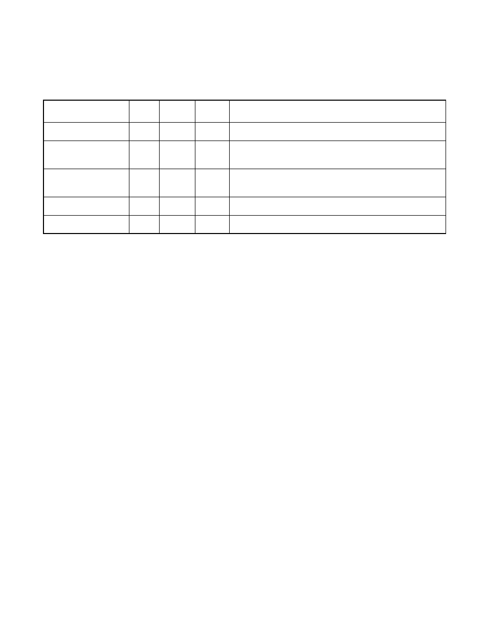
lists and describes the LSI53C140 interface control pins.
Table 3.3
Chip Interface Control Pins
Name
Pin
Ball
Type
Description
RESET/
146
A7
I
Master Reset for LSI53C140, active LOW.
WS_ENABLE/
150
B5
I
Enable/disable SCSI transfers through the
LSI53C140.
XFER_ACTIVE
149
A6
O
Transfers through the LSI53C140 are
enabled/disabled.
CLOCK
147
C8
I
Oscillator input for LSI53C140 (40 MHz).
BSY_LED
148
B6
O
SCSI activity LED output, 8 mA.
Advertising