Avago Technologies LSI53C810AE User Manual
Avago Technologies Hardware
1
Addendum to the SYM53C810A
Data Manual Version 2.0
December, 1997
This addendum contains new and changed information for the SYM53C810A Data Manual
Version 2.0, published in August 1996. The information will be added to the next version of the
manual. The changes are listed in the order in which their appropriate chapters appear in the data
manual. The Power Management features of the SYM53C810AE enable it to comply with
Microsoft’s PC 97 Hardware Design Guide. This addendum applies to both devices,
SYM53C810A and SYM53C810AE, except where noted.
Chapter 2, Functional Description
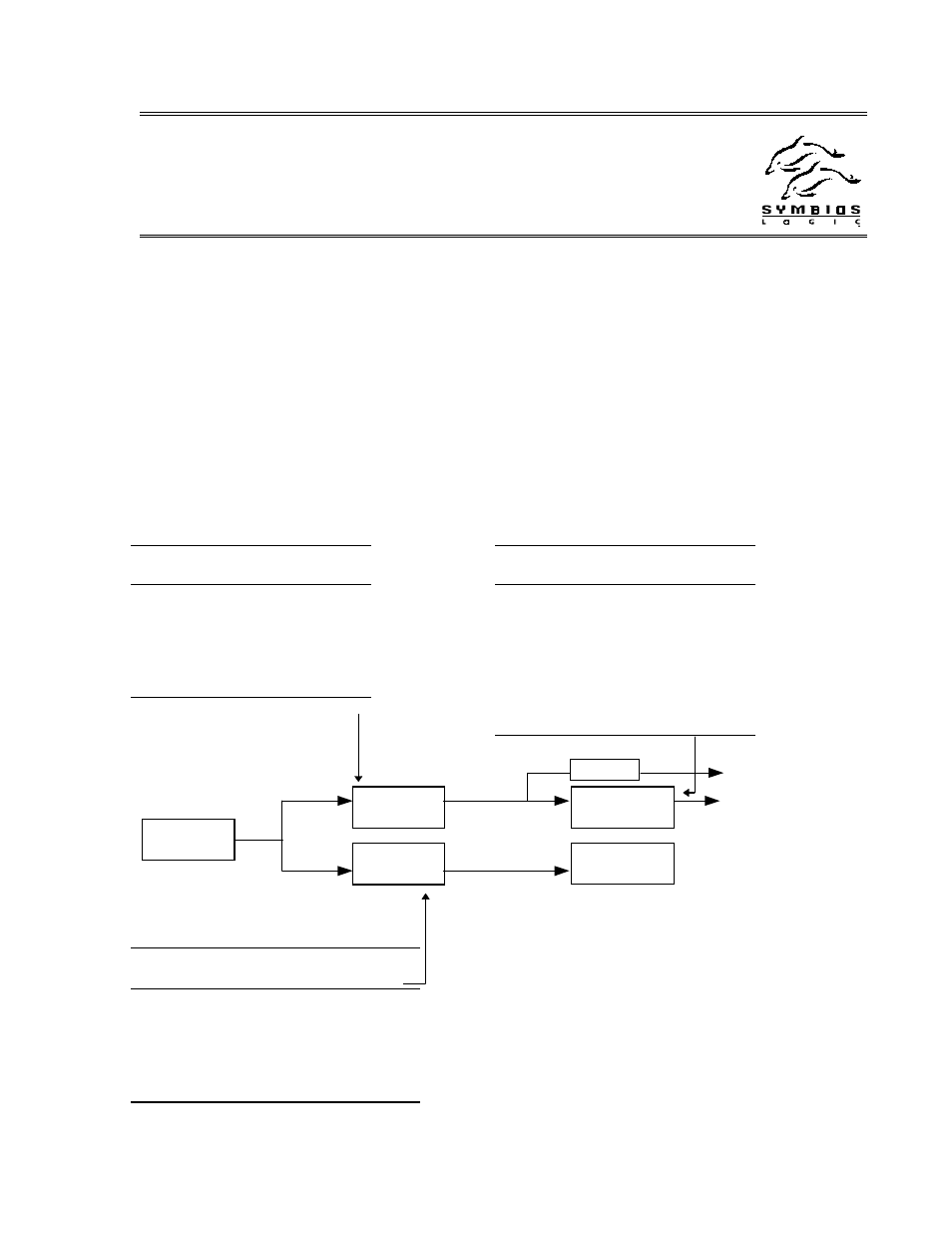
Figure 2-4, “Determining the Synchronous Transfer Rate,” was inadvertently omitted. See the
reference to this figure under the main heading “Synchronous Operation.” The
drawing appears
below.
SCF2
SCF1
SCF0
SCF
Divisor
0
0
1
1
0
1
0
1.5
0
1
1
2
1
0
0
3
0
0
0
3
TP2
TP1
TP0
XFERP
Divisor
0
0
0
4
0
0
1
5
0
1
0
6
0
1
1
7
1
0
0
8
1
0
1
9
1
1
0
10
1
1
1
11
S C L K
S C F
Divider
C C F
Divider
This point
must not
exceed 50
M H z
S y n c h r o n o u s
Divider
A s y n c h r o n o u s
S C S I L o g i c
Divide by 4
Receive
Clock
Send Clock
(to SCSI bus)
CF2
CCF1
CCF0
SCSI Clock
(MHz)
0
0
0
50.1-66.00
0
0
1
16.67-25.00
0
1
0
25.01-37.50
0
1
1
37.51-50.00
1
0
0
50.01-66.00
Example:
SCLK= 40 MHz, SCF = 1(/1), XFERP = 0(/4),
CCF = 3(37.51-50.00MHz)
Synchronous send rate = (SCLK/SCF)/XFERP =
(40/1)/4=10MB/s
Synchronous receive rate = (SCLK/SCF)/4 =
(40/1)/4=10MB/s
Figure 2-4: Determining the Synchronous Transfer
Rate