Pex8605, 12 pci express reference clock outputs – Avago Technologies PEX 8605 User Manual
Page 10
PEX8605
© PLX Technology, www.plxtech.com
Page 10 of 13
2 May 2013, version 1.7
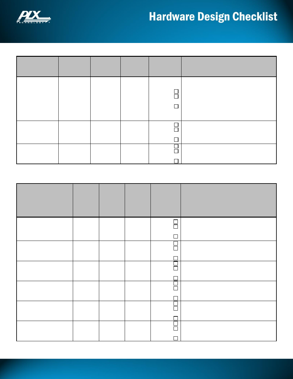
Signal Name
Dual-Row
QFN Pkg.
Pin #
TQFP
Package
Pin #
Signal
Type
Checked
Recommendations
PWRON_RST#
B14
29
I/O
PU
YES
NO
UNKNOWN
Power-On Reset
When stand-by (Vaux) power is implemented, and
where remote wake up using WAKE# or
beacon signaling from D3cold power state has to be
forwarded, PWRON_RST# must be held high when
device is in D3cold power state.
If stand-by power is not implemented, connect this
signal to PEX_PERST#.
WAKE#
B56
128
OD
YES
NO
UNKNOWN
PCI Express WAKE#
If VAUX_IO power rail is implemented, WAKE#
signal should be externally pulled high to
VAUX_IO. Otherwise, pull high to VDD_IO.
XTAL_IN
B30
68
I/O
PU
YES
NO
UNKNOWN
Factory Test Only
Pull or tie directly to Ground.
2.12 PCI Express Reference Clock Outputs
Signal Name
Dual-
Row
QFN
Pkg.
Pin #
TQFP
Package
Pin #
Signal
Type
Checked
Recommendations
PEX_REFCLK_OUTp1
A24
45
HCSLOUT
YES
NO
UNKNOWN
Positive Half of Reference Clock Output Pair 1
Note: No termination resistor networks are required
for REFCLK output pairs.
PEX_REFCLK_OUTn1
B21
46
HCSLOUT
YES
NO
UNKNOWN
Negative Half of Reference Clock Output Pair 1
PEX_REFCLK_OUTp2
A22
41
HCSLOUT
YES
NO
UNKNOWN
Positive Half of Reference Clock Output Pair 2
PEX_REFCLK_OUTn2
A23
43
HCSLOUT
YES
NO
UNKNOWN
Negative Half of Reference Clock Output Pair 2
PEX_REFCLK_OUTp3
A20
38
HCSLOUT
YES
NO
UNKNOWN
Positive Half of Reference Clock Output Pair 3
PEX_REFCLK_OUTn3
A21
39
HCSLOUT
YES
NO
UNKNOWN
Negative Half of Reference Clock Output Pair 3