Cio-dda06/jr block diagram – Measurement Computing CIO-DDA06/JR User Manual
Page 7
Advertising
CIO-DDA06/JR User's Guide
Introducing the CIO-DDA06/JR
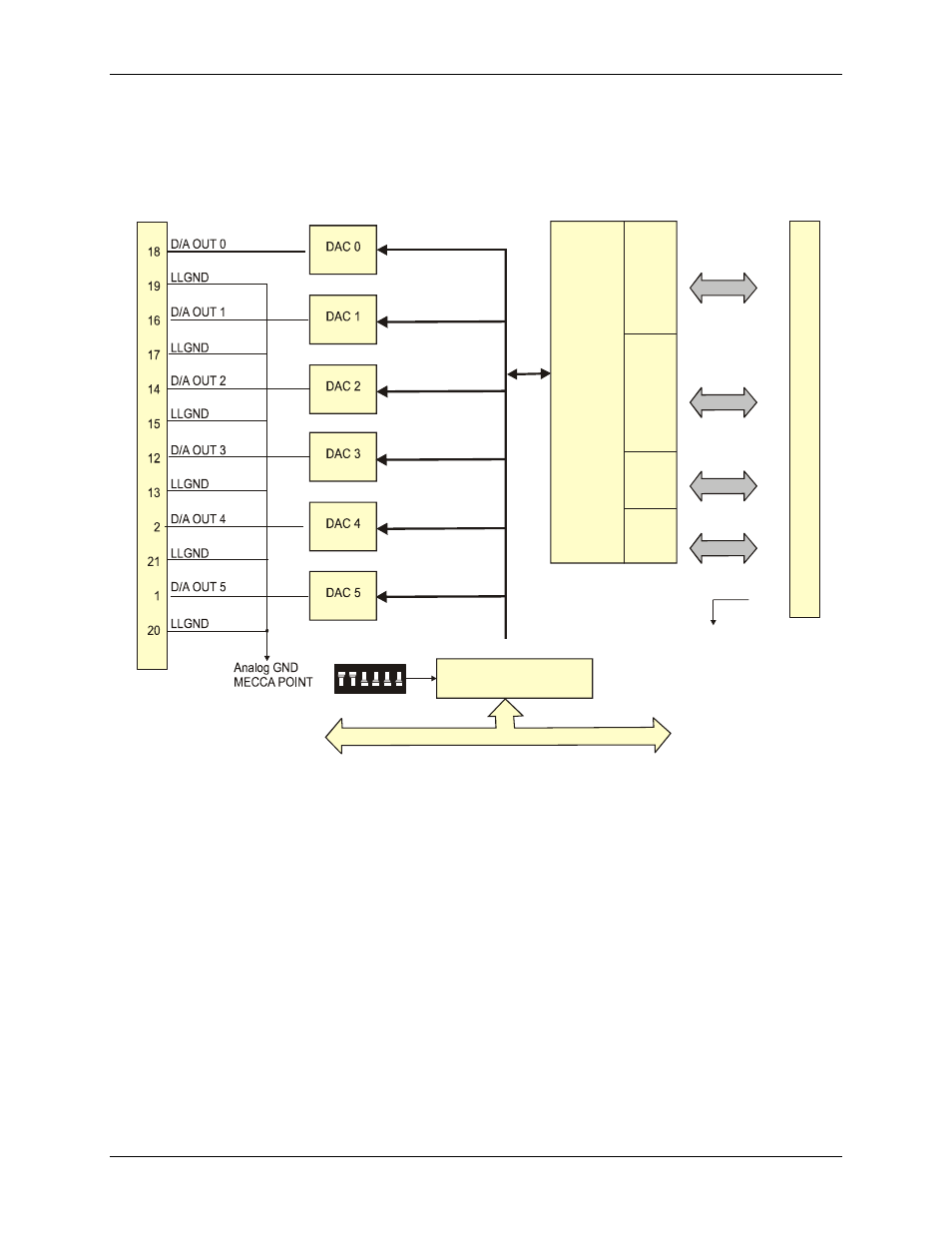
CIO-DDA06/JR block diagram
CIO-DDA06/JR functions are illustrated in the block diagram shown here.
Data
Path
and
Control
High Drive Digital I/O
9 8 7 6 5 4
ADDRESS
FI
RS
TP
O
R
TA
FI
R
S
TP
O
R
TB
FIRSTPORTA Bit 0
Bit 1
Bit 2
Bit 3
Bit 4
Bit 5
Bit 6
Bit 7
FIRSTPORTB Bit 0
Bit 1
Bit 2
Bit 3
Bit 4
Bit 5
Bit 6
Bit 7
FIRSTPORTC Bit 0
Bit 1
Bit 2
Bit 3
FIRSTPORTC Bit 4
Bit 5
Bit 6
Bit 7
DGND
P/O
37-pin D conn.
37
36
35
34
33
32
31
30
10
9
8
7
6
5
4
3
29
28
27
26
25
24
23
22
11
Note: Digital I/O
pin assignments are
the same as for
the CIO-DIO24
ISA Bus
Address Decode
Bus Interface
AD7237KN
P/O
37-pin D conn.
FI
R
ST
PO
RT
C
LO
FI
R
ST
P
O
RTC HI
Works like
8255 mode 0
AD7237KN
AD7237KN
AD7237KN
AD7237KN
AD7237KN
Figure 1. CIO-DDA06/JR Functional block diagram
7
Advertising