2 digital data registers – Measurement Computing PC104-AC5 User Manual
Page 11
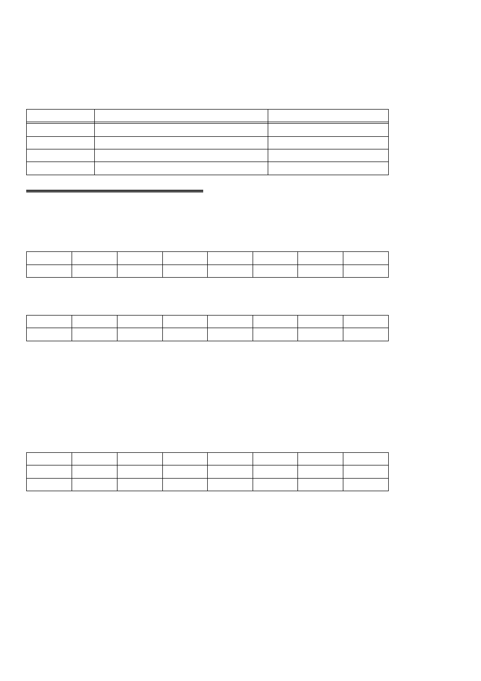
In summary form, the registers and their function are listed on the following table.
Within each register are eight bits which may constitute a byte of data or eight
individual bit set/read functions.
Table 3-1. Board Register Functions
Configure I/O
None.
BASE +3
1st Port C Output
1st Port C Input
BASE +2
1st Port B Output
1st Port B Input
BASE +1
1st Port A Output
1st Port A Input
BASE +0
WRITE FUNCTION
READ FUNCTION
ADDRESS
3.2 DIGITAL DATA REGISTERS
Port A
Base Address + 0
A0
A1
A2
A3
A4
A5
A6
A7
0
1
2
3
4
5
6
7
Port B Data
Base Address +1
B0
B1
B2
B3
B4
B5
B6
B7
0
1
2
3
4
5
6
7
Ports A & B may be programmed as input or output. Each is written to and read from
in bytes, but for control and monitoring, use individual bits.
When using bit set/reset and bit read functions, unwanted bits must be masked out of
reads and ORed into writes.
Port C Data
Base Address +2
CL0
CL1
CL2
CL3
CH0
CH1
CH2
CH3
C0
C1
C2
C3
C4
C5
C6
C7
0
1
2
3
4
5
6
7
Port C may be used as one 8-bit port of either input or output, or it may be split into
two 4-bit ports which may be independently input or output. The notation for the
upper 4-bit port is CH3 - CH0, and for the lower, CL3 - CL0.
Although it may be split, every read and write to port C carries eight bits of data so
unwanted information must be ANDed out of reads, and writes must be ORed with the
current status of the other port.
7