Pci-das08 block diagram, Pci-das08 block diagram -2, Pci-das08 user's guide introducing the pci-das08 – Measurement Computing PCI-DAS08 User Manual
Page 8: Figure 1-1. pci-das08 block diagram
Advertising
PCI-DAS08 User's Guide
Introducing the PCI-DAS08
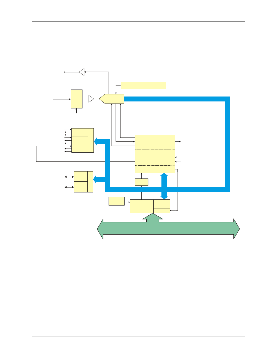
PCI-DAS08 block diagram
PCI-DAS08 functions are illustrated in the block diagram shown here.
PCI
Controller
BADR1
Interrupt
Boot
EEPROM
Counter 2
Clock
(33 MHz/8)
Interrupt
Control
Decode/Status
Bus
Timing
Channel Select
Output Clock2
EXT_INT
Controller FPGA and Logic
LOCAL BUS
PCI BUS (5 V, 32-BIT, 33 MHZ)
Input
Port
C
ont
ro
l
Input (2:0)
Digital I/O
82C54
16-bit Counters
Input Clock2
Counter 0
Co
n
tr
o
l
Counter 1
Counter 2
Input Clock0
Gate0
Output Clock0
Input Clock1
Gate1
Output Clock1
Gate2
Output Clock2
Output
Port
Output (3:0)
ADC and MUX
Control
10 Volt
Reference
Channel Select
Gain and Offset Cal
Mux
Analog In
8 CH S.E.
Buffer
12-bit, 100 kHz
Start EOC
Buffer
BADR2
A/D
Control
Figure 1-1. PCI-DAS08 block diagram
1-2
Advertising