Measurement Computing PCI-DAS4020/12 User Manual
Page 19
Advertising
PCI-DAS4020/12 User's Guide
Functional Details
19
Solder Gap Configuration
Input Impedance
Open
1.5 M typical
Close
50
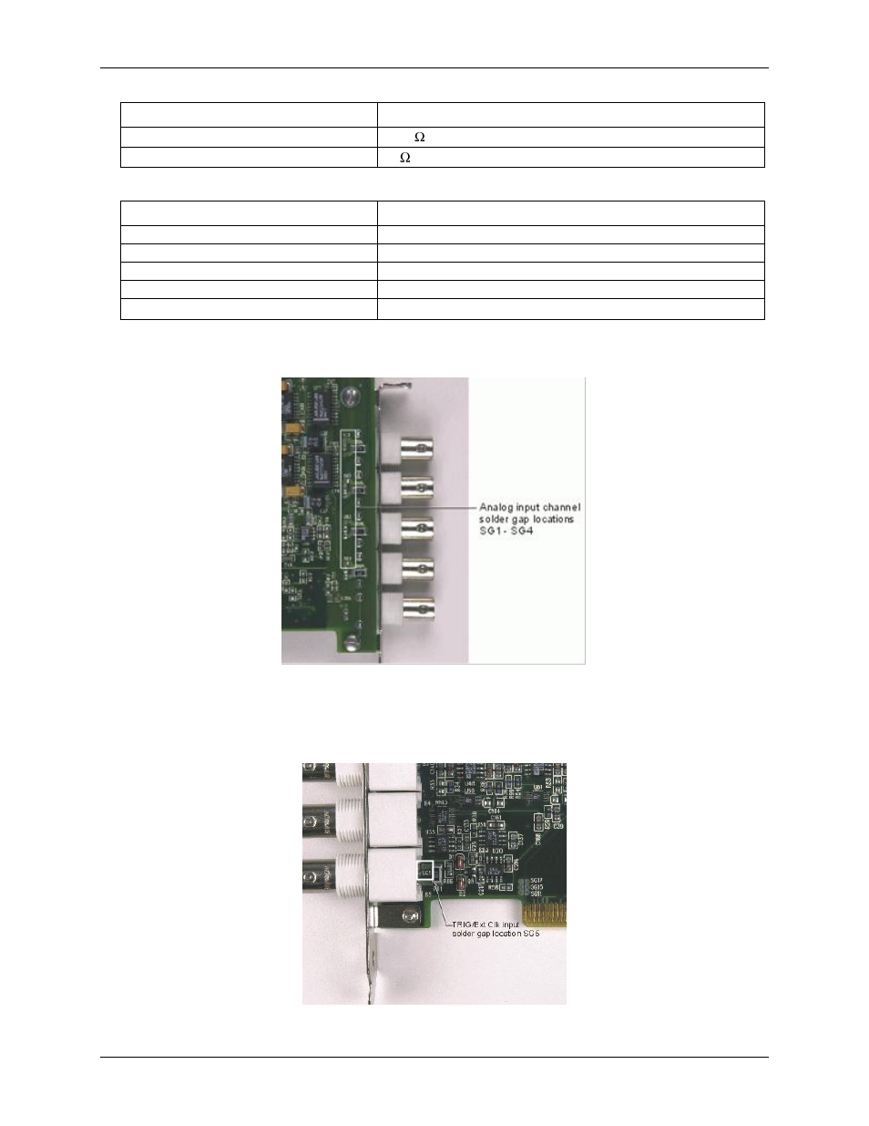
The board designation for the analog input channels and the trigger/clock BNC input are listed below.
Solder Gap board label
Channel
SG1
Channel 0
SG2
Channel 1
SG3
Channel 2
SG4
Channel 3
SG5
TRIG/Ext Clock
input
Solder gaps for the analog input channels are located on the rear of the board (circuit-side) and are labeled
SG1
to
SG4
Figure 10. Analog input channel solder gap locations (circuit-side)
The solder gap for the trigger/clock input is located on the front of the board (component-side) and is labeled
SG5
. See Figure 11.
Figure 11. Trigger/clock input solder gap location (component-side)
Advertising