Output signal descriptions pcb requirements – MicroE CE300 ChipEncoder User Manual
Page 7
Miscellaneous Application Notes
The printed circuit board (PCB) land pattern and assembly processes necessary to successfully integrate the CE300’s Ball Grid Array (BGA) package are
detailed as follows:
• IPC-SM-782 (land pattern standard) should be used as a guide for proper land pattern design for the solder pads on the printed
circuit board.
• Due to the tight spacing between solder pads, it is recommended that there be solder mask between the solder pads to prevent
solder bridging and shorting to adjacent pads.
• A stainless steel stencil, 0.003 inch [0.08 mm] thick is recommended for solder paste application to the printed
circuit board lands.
• Machine placement and reflow soldering of the CE300 is preferred. If hand soldering is necessary, soldering to the castellations
should be done noting precautions in the preceding section of this manual.
• Acetone is the recommended cleaner for the CE300.
Output Signal Descriptions
PCB Requirements
The CE300 electrical interface, land pattern, schematic of additional required passive components and mechanical dimensions are found in the CE300’s interface
drawings. See page 5 for instructions on downloading interface drawings.
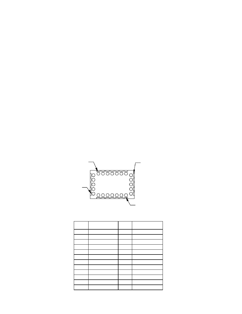
Bottom view of ChipEncoder
Page 7
Pad Function
Pad Function
1
Index Window+
13
AN
2
GND
14
Sin+
3
RESERVED
15
RESERVED
4
RESERVED
16
RESERVED
5
CP+
17
RESERVED
6
+5VA
18
GND
7
RESERVED
19
+5VD
8
GND
20
B+
9
DC2
21
B-
10
RESERVED
22
A+
11
DC1
23
A-
12
RESERVED
24
Index Window+
PAD 1
PAD 20
PAD 8
PAD 13