Functional description, Receive circuit, Fpga – Grass Valley 8914 User Manual
Page 14
8
8914 Instruction Manual
8914 Dual AES/EBU Delay Distribution Amplifier
Functional Description
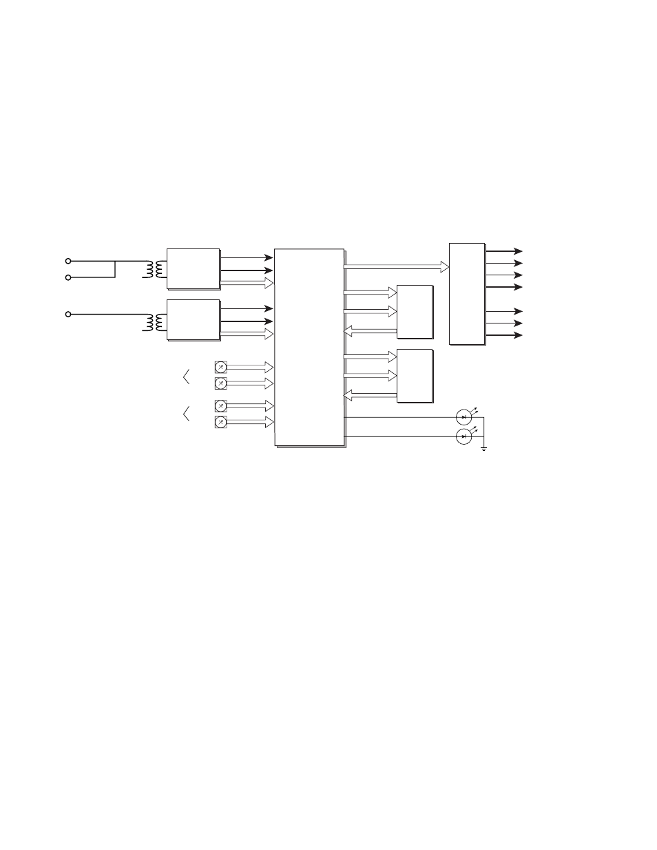
Refer to the block diagram in
while reading the description.
There are 2 inputs for the module. One of these inputs is a loop-through
input. The data paths are otherwise conceptually identical for both inputs.
The inputs are first received by the receive circuit. Next, the Field Program-
mable Gate Array (FPGA) sends the data to the FIFO, which returns the
data to the FPGA. Finally, the data is passed to the transmit circuit.
Figure 5. 8914 Dual AES/EBU Delay DA Block Diagram
Receive Circuit
This circuit features a digital audio transformer conforming to EBU stan-
dards.
The AES/EBU receiver recovers audio data and low jitter clocks from the
digital audio input transmission line. The data is reclocked, and then sent
to the FPGA. A special mode allows the preamble and bi-phase mark data
to pass through in its entirety. The 6.144 MHz clock signal is also sent to the
FPGA.
FPGA
The FPGA is a field programmable gate array containing proprietary Grass
Valley control circuitry. The FPGA converts the serial AES/EBU stream to
12-bit parallel data. The width of the data corresponds to the width of the
Delay 1
Delay Select Switches
0547-01
AES/EBU
Receiver
Field
Programmable
Gate Array
(FPGA)
Coarse
Fine
Coarse
Fine
Control
Clock
Serial Data
Control
Control
Clock
AES Input 1
AES Outputs
Serial Data
Parallel Data
Parallel Data
Control
Parallel Data
Parallel Data
Lock Ch. 1
Lock Ch. 2
AES/EBU
Receiver
Delay 2
AES Input 2
FIFO
FIFO
Line
Drivers
(Transmit)
Delay
1
Delay
2
Loop-through