Jumper settings, Jumper settings 10, Chapter 3 – Lanner LEC-3110 User Manual
Page 12: Motherboard information
10
Motherboard Information
Chapter 3
Embedded and Industrial Computing
Jumper Settings
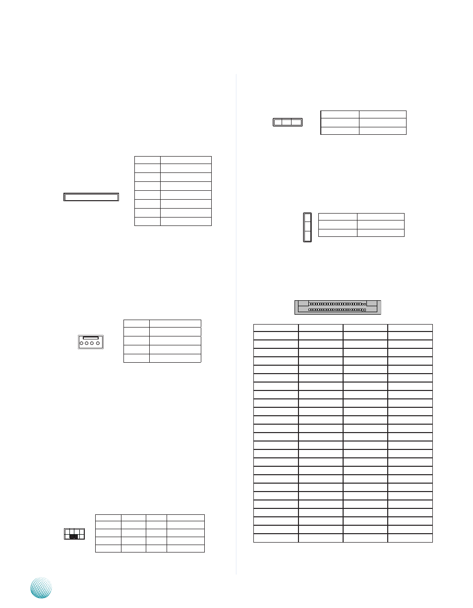
SATA Connector (J10, J11): The system supports one
SATA drive with a transfer rate of 3 0 Gb/s This port
support both SATA and SATA DOM and detects between
them automatically
SATA Power Connector (J3): Connect the 4-pin SATA
power connector to this port
Keyboard and mouse interface Connectors(J7): It is
for connecting the PS/2 keyboard and mouse interface
cable
Clear CMOS jumper (JP2): It is for clearing the CMOS
memory and system setup parameters by erasing the data
stored in the CMOS RAM such as the system passwords
CompactFlash Primary/Slave Selection Jumper (JP1):
The system’s CompactFlash connects to LEC-3110’s
Primary IDE port in parallel with a reserved IDE connector
This jumper configures the CF socket to be the Master
(default) or Slave IDE device
CompactFlash Connector (CN2): It is for connecting a
Compact Flash card to be served as your system’s storage
The connector is a CF Type II slot which could fit both CF
Type I or CF Type II cards
Pin No.
Function
Pin No.
Function
1
GND
26
CF_CD1#
2
CF_DD3
27
CF_DD11
3
CF_DD4
28
CF_DD12
4
CF_DD5
29
CF_DD13
5
CF_DD6
30
CF_DD14
6
CF_DD7
31
CF_DD15
7
CF_DCS0#
32
CF_DCS1#
8
A10(GND)
33
VS1#
9
OE#(GND)
34
CF_DIOR#
10
A9(GND)
35
CF_DIOW#
11
A8(GND)
36
WE#(VCC3)
12
A7(GND)
37
CF_IRQ#
13
VCC
38
VCC
14
A6(GND)
39
CSEL#(GND)
15
A5(GND)
40
VS2#
16
A4(GND)
41
CF_RESET#
17
A3(GND)
42
CF_IORDY
18
CF_A2
43
CF_DMARQ
19
CF_A1
44
CF_DDACK#
20
CF_A0
45
CF_ACT#
21
CF_DD0
46
CF_DIAG
22
CF_DD1
47
CF_DD8
23
CF_DD2
48
CF_DD9
24
WP(NC)
49
CF_DD10
25
CF_CD2#
50
GND
Pin No.
Function
1
GND
2
TX+
3
TX-
4
GND
5
RX-
6
RX+
7
5V
Pin No.
Function
1-2
Normal (Default)
2-3
Clear CMOS
3 2 1
Pin No.
Function
1
VCV12 (12V)
2
GND
3
GND
4
VCC (5V)
Pin No.
Function
1-2
Master (Default)
2-3
Slave
1
2
3
25 1
50 26
Pin No.
Function
Pin No.
Function
1
VCC
2
MSCLK
3
MSDAT
6
KEY
5
KBDAT
6
KEY
7
GND
8
KBCLK
7 6 5 4 3 2 1
1 2 3 4
2 4 6 8
1 3 5 7