Chapter 2, System information, Block diagram: the mainboard – Lanner LEC-7388S User Manual
Page 7
7
System Information
Chapter 2
Embedded and Industrial Computing
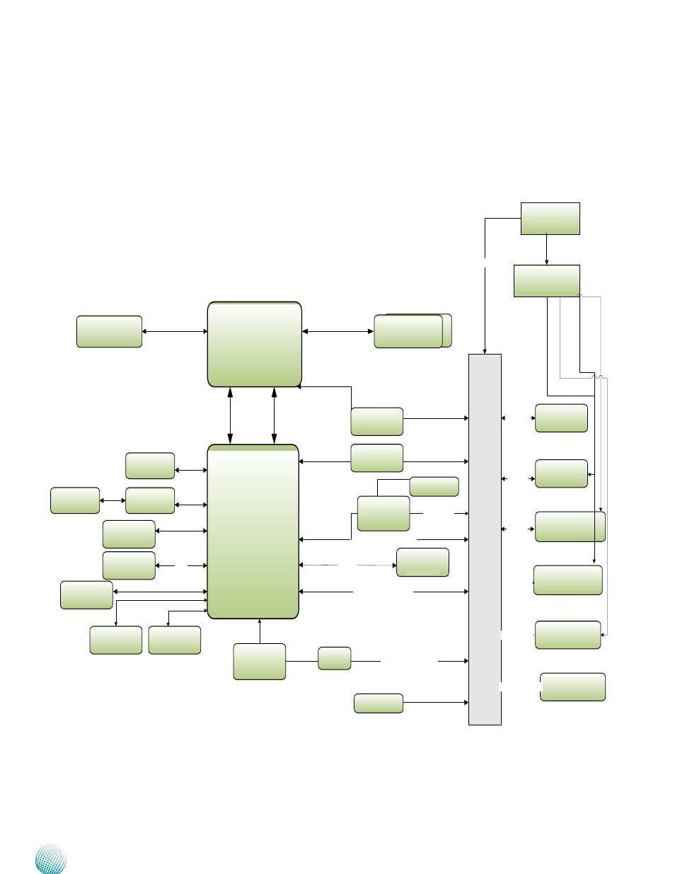
Block Diagram: The MainBoard
The block diagram depicts the relationships among the
interfaces and modules on the motherboard.
Mobile
Intel QM87
Chipset
4th
Generation
Intel Core
I5-4400E
DDR III
SODIMM B
DMI
DDR3
PCIex1
Giga LAN
PHY
IntelR i210
F
D
I
2 x SO-DIMM
Sockets
(Dual channel)
3 x USB2.0/1 x USB3.0
TMDS
Control Signal (UART)
Super I/O
JAE TX25
80-Pin
Connector
USB
PCIe
Serial
Port
2 x Realtek
ALC886
Codec
Line-In/
MIC
Audio
L/R channel
DC Input
+12
HDMI
Display Port
BIOS
Support
1x SATA
Port
2x Type-A
USB 3.0
External
2.5" Driv
Mini-PCIe
Socket
LED
Power-ON
Reset
Intel High Definition Audio
Audio Jack
output
USB 3.0 Port
USB 2.0 Type A
dual port
Display Port
HDMI Port
2 x5 Terminal
Block
Audio Out
USB 3.0
USB 2.0
Display Port
HDMI Signal
RS-232 (TX, RX)
DC-DC
Converter
DC-IN from
Power
Adaptor
DC +12V IN
Intel i217