Absolute maximum ratings, Performance data, Supply rx data pdn rx data – Linx Technologies RXD-xxx-KH2 User Manual
Page 2: No rfin rfin >-35dbm
Page 3
Page 2
ABSOLUTE MAXIMUM RATINGS
Supply Voltage V
CC
-0.3
to
+3.6
VDC
Supply Voltage V
CC
, Using Resistor
-0.3
to
+5.2
VDC
Any Input or Output Pin
-0.3
to
+3.6
VDC
RF Input
0
dBm
Operating Temperature
-30
to
+70
°C
Storage Temperature
-45
to
+85
°C
Soldering Temperature
+225°C for 10 seconds
*NOTE*
Exceeding any of the limits of this section may lead to permanent
damage to the device. Furthermore, extended operation at these maximum
ratings may reduce the life of this device.
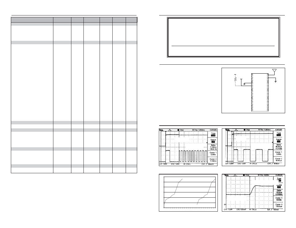
PERFORMANCE DATA
These performance parameters
are based on module operation at
25°C from a 3.0VDC supply unless
otherwise noted. Figure 2
illustrates the connections
necessary for testing and
operation. It is recommended all
ground pins be connected to the
ground plane. The pins marked NC
have no electrical connection and
are designed only to add physical
support.
Figure 2: Test / Basic Application Circuit
NC
D0
D1
GND
VCC
PDN
D2
D3
D4
DATA
VT
D5
ANT
GND
NC
RSSI
A9
A8
A7
A6
A5
A4
A3
A2
D6
A1
D7
A0
1
2
3
4
5
6
7
8
9
10
11
28
27
26
25
24
23
22
21
20
19
18
17
16
15
12
13
14
3VDC
5VDC
330
Ω
External
Resistor
TYPICAL PERFORMANCE GRAPHS
ELECTRICAL SPECIFICATIONS
1. The KH2 can utilize a 4.3 to 5.2VDC supply provided a 330-ohm resistor is placed in series with VCC.
2. Into a 50-ohm load.
3. When operating from a 5V source, it is important to consider that the output will swing to well less than
5 volts as a result of the required dropping resistor. Please verify that the minimum voltage will meet the
high threshold requirement of the device to which data is being sent.
4. For BER of 10-5 at 1,200bps.
5. Characterized, but not tested.
6. Time to valid data output.
7. Maximum drive capability of data outputs.
Notes
Table 1: KH2 Series Receiver Specifications
Parameter
Designation
Min.
Typical
Max.
Units
Notes
POWER SUPPLY
Operating Voltage
V
CC
2.7
3.0
3.6
VDC
–
With Dropping Resistor
4.3
5.0
5.2
VDC
1,5
Supply Current
I
CC
4.0
5.2
7.0
mA
–
Power-Down Current
I
PDN
20.0
28.0
35.0
µA
5
RECEIVER SECTION
Receive Frequency Range:
F
C
RXD-315-KH2
–
315
–
MHz
–
RXD-418-KH2
–
418
–
MHz
–
RXD-433-KH2
–
433.92
–
MHz
–
Center Frequency Accuracy
–
-50
–
+50
kHz
–
LO Feedthrough
–
–
-80
–
dBm
2,5
IF Frequency
F
IF
–
10.7
–
MHz
5
Noise Bandwidth
N
3DB
–
280
–
kHz
–
Data Rate
–
100
–
10,000
bps
–
Data Output:
Logic Low
V
OL
–
0.0
–
VDC
3
Logic High
V
OH
–
3.0
–
VDC
3
Power-Down Input:
Logic Low
V
IL
–
–
0.4
VDC
–
Logic High
V
IH
V
CC
-0.4
–
–
VDC
–
Receiver Sensitivity
–
-106
-112
-118
dBm
4
RSSI / Analog:
Dynamic Range
–
–
80
–
dB
5
Analog Bandwidth
–
50
–
5,000
Hz
5
Gain
–
–
16
–
mV / dB
5
Voltage With No Carrier
–
–
1.5
–
V
5
ANTENNA PORT
RF Input Impedance
R
IN
–
50
–
Ω
5
TIMING
Receiver Turn-On Time:
Via V
CC
–
3.0
7.0
10.0
mSec
5,6
Via PDN
–
0.04
0.25
0.50
mSec
5,6
Max. Time Between Transitions
–
–
10.0
–
mSec
5
DECODER SECTION
TX Data Length
–
–
26 bits 3x
–
–
–
Average Data Duty Cycle
–
–
50%
–
–
–
Decoder Oscillator
F
ENC
–
70
–
kHz
–
Output Drive Current
–
0.6
1.0
1.2
mA
7
ENVIRONMENTAL
Operating Temperature Range
–
-40
–
+70
°
C
5
Figure 3: Turn-On Time from V
CC
Figure 4: Turn-On Time from PDN
Supply Current (mA)
Supply Voltage (VDC)
5.10
5.15
5.20
5.25
5.30
5.35
5.40
2.7 2.8 2.9 3.0 3.1 3.2 3.3 3.4 3.5 3.6 3.7 3.8 3.9 4.0 4.1 4.2 4.3 4.4 4.5 4.6 4.7 4.8 4.9 5.0 5.1 5.2
With Dropping
Resistor
Figure 5: Consumption vs. Supply
Figure 6: RSSI Response Time
Supply
RX Data
PDN
RX DATA
NO RFIN
RFIN >-35dBm