Typical performance graphs, Absolute maximum ratings, Electrical specifications – Linx Technologies RXM-900-HP3-xxx User Manual
Page 2: Performance data
Page 3
-110
-100
-90
-80
-70
-60
-50
-40
1.0
1.5
2.0
2.5
3.0
RF INPUT (dBm)
RSSI VOLTAGE (V)
Figure 5: Worst Case RSSI Response Time
Figure 3: RX Enabled to Valid Data
Figure 6: BER vs. Input Power (typical)
CH1 500mV
1
Delta 4.080mS
1mS
RX OFF
RX ON >-35dBm
10
-6
10
-5
10
-4
10
-3
-92 -93 -94 -95 -96 -97 -98 -99 -100
-101
-102
BER
PIN (dBm)
Figure 4: Receiver RSSI
TYPICAL PERFORMANCE GRAPHS
Page 2
CH1 1.00V
CH2 2.00V
500uS
1
2
PDN
RX DATA
Delta 1.920mS
ABSOLUTE MAXIMUM RATINGS
Supply Voltage V
CC
-0.3
to
+18.0
VDC
Any Input or Output Pin
-0.3
to
V
CC
VDC
Operating Temperature
-30
to
+85
°C
Storage Temperature
-45
to
+85
°C
Soldering Temperature
+260°C for 10 seconds
*NOTE*
Exceeding any of the limits of this section may lead to permanent
damage to the device. Furthermore, extended operation at these maximum
ratings may reduce the life of this device.
ELECTRICAL SPECIFICATIONS
Parameter
Designation
Min.
Typical
Max.
Units
Notes
POWER SUPPLY
Operating Voltage
V
CC
2.8
3.0
13.0
VDC
–
Supply Current
I
CC
16.0
19.0
21.0
mA
1
Power-Down Current
I
PDN
–
5.6
10.0
µA
2
RECEIVE SECTION
Receive Frequency Range
F
C
902.62
–
927.62
MHz
3
Center Frequency Accuracy
-50
+50
kHz
Channel Spacing
–
–
250
–
kHz
3
First IF Frequency
–
34.7
–
MHz
4
Second IF Frequency
–
10.7
–
MHz
4
Noise Bandwidth
N
3DB
–
280
–
kHz
–
Data Rate
–
100
–
56,000
bps
–
Analog / Audio Bandwidth
–
50
–
28,000
Hz
4
Analog / Audio Output Level
0.8
1.1
2.0
VAC
5
Data Output:
Logic Low
–
0.0
–
0.5
VDC
6
Logic High
–
V
CC
-0.3
–
V
CC
VDC
6
Output Impedance
–
17
–
kohms
–
Data Output Source Current
–
230
–
µA
7
Receiver Sensitivity
-94
-100
-107
dBm
8,9
RSSI:
Dynamic Range
60
70
80
dB
4
Gain
–
24
–
mV/dB
4
Voltage With No Carrier
–
–
1.6
V
4
Spurious Emissions
–
-57
–
dBm
4
Interference Rejection:
FC±1MHz
–
54
–
dB
4
FC±5MHz
–
57
–
dB
4
ANTENNA PORT
RF Input Impedance
R
OUT
–
50
–
Ω
4
TIMING
Receiver Turn-On Time:
via V
CC
T4
–
–
7.0
mSec
4
via PDN
T3
–
–
3.0
mSec
4
Channel Change Time
T2
–
–
1.5
mSec
4
Max time between transitions
T1
–
–
20
mSec
4
ENVIRONMENTAL
Operating Temperature Range
–
-30
–
+85
°
C
4
1. Over the entire operating voltage range.
2. With the PDN pin low.
3. Serial
mode.
4. Characterized, but not tested.
5. With 1kHz sine wave @ 115kHz transmitter deviation
6. No load.
7. With 1V output drop.
8. For 10
-5
@ 9,600bps.
9. At specified center frequency.
Notes
Table 1: HP3 Series Receiver Specifications
PERFORMANCE DATA
These performance parameters
are based on module operation at
25°C from a 3.0VDC supply unless
otherwise noted. Figure 2
illustrates the connections
necessary for testing and
operation. It is recommended all
ground pins be connected to the
ground plane. The pins marked NC
have no electrical connection.
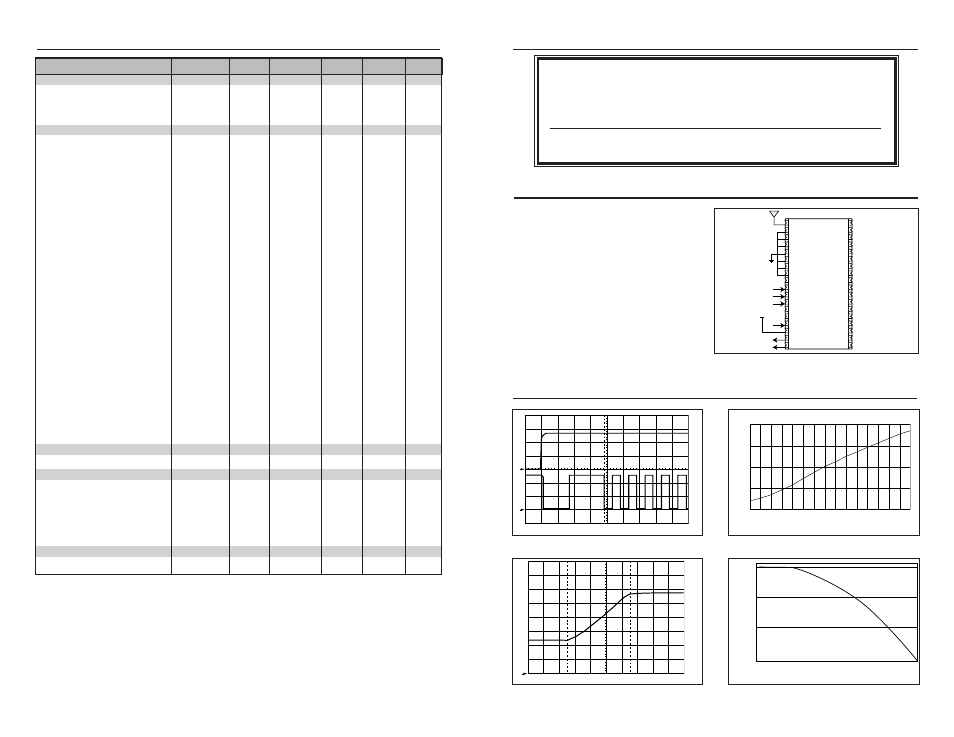
Figure 2: Test / Basic Application Circuit
ANT
GND
GND
NC
NC
NC
NC
NC
NC
GND
GND
GND
GND
GND
NC
NC
NC
CS0
CS1 / SS CLOCK
NC
NC
NC
NC
CS2 / SS DATA
PDN
RSSI
NC
NC
MODE
VCC
AUDIO
NC
NC
DATA
NC
NC
5VDC
PC
PC
PC
PC