The prototyping area, Host interface module – Linx Technologies MDEV-900-HP3-xxx User Manual
Page 4
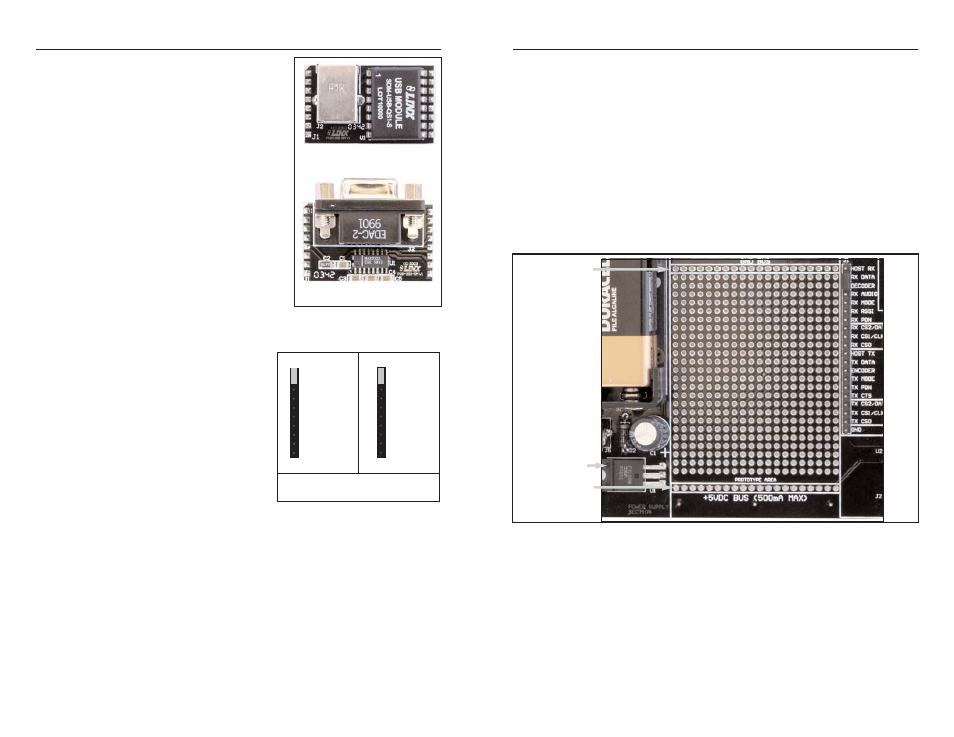
THE PROTOTYPING AREA
A designer wishing to use the development board for product prototyping may
route the necessary signals from the development board's breakout header to
the prototyping area and then use this to build the custom circuitry.
J1 is a wire-wrap header that is provided as an easy access point to the module's
signals. The header pins extend through the board to allow wire attachment on
the back of the board.
Regulated power connections are available on the buses labeled "GND" and
"+5VDC". The board also has a DC power jack to allow powering from an
external power supply rather than with the battery. This jack accepts a 5.5mm
plug with the tip ground and the outer shell 7-16VDC positive supply.
NOTE: The on-board 5-volt regulator has approximately 500mA of headroom
available for user's circuitry. If additional current capacity is required, the user
must add an additional regulator to the prototyping area or power the board from
an external supply.
Page 7
Page 6
HOST INTERFACE MODULE
The HP3 Master Development System features
a Host Interface socket, which allows the use of
two different PC interface modules. The first is a
USB interface module that uses a standard USB
cable (not included) to connect to a PC’s USB
port or a USB hub. The second type of module
is a RS-232 interface module that can be
connected to a standard serial COM port on a
PC using a straight-through 9-pin extension
cable (not included). The evaluation board is
considered a DCE device and as such is
designed to be connected using a straight-thru
serial extension cable. Do not use a null-modem
cable as the boards will not function.
To install, select the module to be used and then
line up the pins on the module with the headers
on the board. Verify that the pin one polarity
marks on the board and on the Host Interface
Module match. The USB jack or the D-sub
connector should face away from the board.
Press firmly on the module so that it slides fully
into the header.
The development system may be prepared
for host operation with the supplied Linx
software by setting the jumpers on the
header as shown in the adjacent figure. This
routes the module's data lines to the Host
Interface Module. Despite being electrically
interfaced, appropriate protocol must be
employed to ensure reliable and error-free
data transfer since the HP3 Series modules
do not encode or packetize the data in any
manner. It is important to understand that
the development boards are transparent;
that is, the user's software is entirely
responsible for controlling the timing and
error correction aspects of the link. The evaluation boards have no provision to
check or qualify the incoming data. When designing a protocol to transfer data
across a wireless link, it is very important to remember that interference is
inevitable. The protocol must support error detection and correction if it is to be
successful. A correctly designed protocol will provide optimum performance and
throughput for product-specific applications while taking into account the timing
and data-rate requirements of the module. For further information on protocol
considerations please refer to Application Note AN-00160.
If the designer needs to develop protocols using a physical implementation other
than an RS-232 or USB interface, the designer can build the custom interface
circuitry in the prototyping area and route the module's data signals from the
header to the prototyping area.
HOST TX
TX DATA
ENCODER
TX MODE
TX PDN
TX CTS
TX CS2/DATA
TX CS1/CLK
TX CS0
GND
J1
TX
RX
J1
HOST RX
RX DATA
DECODER
RX AUDIO
RX MODE
RX RSSI
RX PDN
RX CS2/DATA
RX CS1/CLK
RX CS0
HOST MODE JUMPER
CONFIGURATION
USB Interface Module
RS232 Interface Module
Figure 4: Host Interface Modules
Figure 6: The Prototyping Area
Ground Bus
Regulator
+5 Volt Bus
Figure 5: Jumper Configuration