Caution, Electrical specifications, Schematic – Linx Technologies ASY-MDEV-GPS-SG-DB User Manual
Page 2: Pin assignments pcb layout
Page 3
GND
NC
NC
VCC
NC
VBACKUP
NC
NC
NC
GND
GND
NC
NC
TXM
RXM
1PPS
GPIO0
RFPWRUP
ON_OFF
GND
Page 2
Figure 1: MDEV-GPS-SG-DB Pin Assignments
ELECTRICAL SPECIFICATIONS
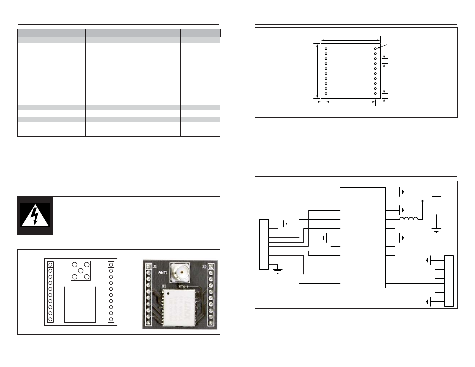
Figure 3: MDEV-GPS-SG-DB Schematic
SCHEMATIC
1
2
3
4
5
6
7
8
9
10
J1
GND
GND
1
2
3
4
5
6
7
8
9
10
J2
GND
GND
RF
GND
ANT1
CONREVSMA001
GND
GND
GND
GND
GND
RXB
1
TXB
2
1PPS
3
TXA
4
RXA
5
GPIO10
6
LCKIND
7
GPIO1
8
RRPWRUP
9
ON_OFF
10
VBACKUP
11
VIN
12
GPIO14
13
GPIO15
14
GPIO13
15
BOOTSEL
16
VOUT
17
GND
18
RFIN
19
GND
20
GND
21
GND
22
U1
RXM-GPS-SG
L1
300ohm BEAD
Table 1: SG Series Receiver Specifications
Parameter
Designation
Min.
Typical
Max.
Units
Notes
POWER SUPPLY
Supply Voltage
V
CC
3.0
–
4.2
VDC
1
Supply Current:
I
CC
2
Peak
–
–
46.0
mA
6
Acquisition
–
32
–
mA
6
Tracking
–
28
–
mA
6
Standby
–
1.5
–
mA
6
Backup Battery Voltage
V
BAT
1.3
–
6.0
VDC
–
Backup Battery Current
I
BAT
–
10
–
µA
–
2.85V Output Voltage
V
OUT
2.79
2.85
2.91
VDC
–
2.85V Output Current
I
OUT
–
–
30
mA
3
ANTENNA PORT
RF Input Impedance
R
IN
–
50
–
Ω
–
ENVIRONMENTAL
Operating Temperature Range
–
-30
–
+85
°
C
–
Storage Temperature Range
–
-40
25
+85
°
C
–
Notes:
1. I
OUT
= 0
2. V
CC
= 3.3V, I
OUT
= 0
3. V
CC
= 3.3V
6. With passive antenna. Active antennas will increase current consumption.
Please see the SG Series GPS Module Data Guide for full specifications,
features and operation instructions.
1.20”
(47.24)
0.10”
(2.54)
0.10”
(2.54)
0.10”
(2.54)
1.10”
(27.94)
1.00”
(25.40)
Ø0.04” x 10
(1.02)
Figure 2: MDEV-GPS-SG-DB PCB Layout Dimensions
PIN ASSIGNMENTS
PCB LAYOUT
*CAUTION*
This product incorporates numerous static-sensitive components.
Always wear an ESD wrist strap and observe proper ESD handling
procedures when working with this device. Failure to observe this
precaution may result in module damage or failure.
The daughter board uses 0.02” diameter round header pins on 0.1” centers.
These headers can be soldered directly to the PCB or plugged into a matching
socket to enable easy removal.