J3 opto and pin out table – Remote Processing RPC-210 User Manual
Page 34

DIGITAL LINES
BASIC
SECTION 6
Page 6-6
Pin out for J7 is shown below.
J7 Pin
No.
Description
Alternate
Function
1
Real time clock interrupt
source
2
Digital input, ad dress
0A400H , bit 6
3
Interr upt 0
4
RTC squar e wave output
5
COM 1 interrupt source
6
Digital input, ad dress
0A400H , bit 5
Keypad row 6
7
Ground
8
+ 5V
9
Exter nal pulse out @
address 0A500H
10
Digital output, a ddress
0A307H
11
Ground
12
RS-232 shut down
control
13
+ 5V
14
SPI data from device
15
Ground
16
SPI data to device
17
Autorun sense
18
SPI clock to device
19
Digital input, ad dress
0A400H , bit 4
Keypad row 5
20
Clock power on strobe.
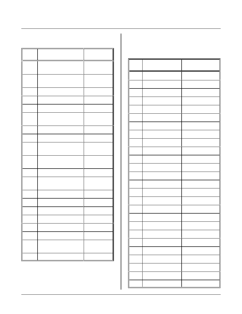
J3 Opto and Pin Out table
This table shows correspondence between J3 pin number
and opto rack channel number.
J3
Pin #
82C55 Descr iption
Accesse d as Opto
channel no.
19
Port A , bit 0
108
21
Port A , bit 1
109
23
Port A , bit 2
110
25
Port A , bit 3
111
24
Port A , bit 4
112
22
Port A , bit 5
113
20
Port A , bit 6
114
18
Port A , bit 7
115
10
Port B, bit 0
116
8
Port B, bit 1
117
4
Port B, bit 2
118
6
Port B, bit 3
119
1
Port B, bit 4
120
3
Port B, bit 5
121
5
Port B, bit 6
122
7
Port B, bit 7
123
13
Port C , bit 0
100
16
Port C , bit 1
101
15
Port C , bit 2
102
17
Port C , bit 3
103
14
Port C , bit 4
104
11
Port C , bit 5
105
12
Port C , bit 6
106
9
Port C , bit 7
107
26
Ground
2
+ 5V