And-tft-25xs-led-kit – Purdy AND-TFT-25XS-LED-KIT User Manual
Page 5
Purdy Electronics Corporation • 720 Palomar Avenue • Sunnyvale, CA 94085
6/27/08
Tel: 408.523.8200 • Fax: 408.733.1287 • [email protected] • www.purdyelectronics.com
5
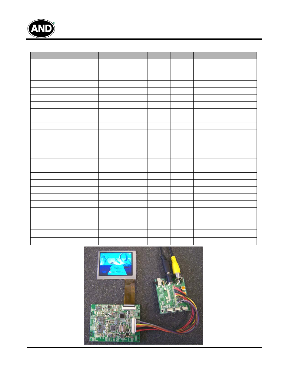
Input/Output Connector, LCD Module Connector, FFC Down Connector, 30 pins Pitch: 0.5 mm
Timing Characteristics of Input SIgnal
Characteristics
Symbol
Min.
Typ.
Max.
Unit
Remarks
1 Field Scanning Period
t1V
–
262.5
–
H
1 Line Scanning Period
t1H
–
63.5
–
µ
s
Source Driver Operating Frequency
fhc
1.0
3.14
5.0
MHz
Signal Sampling Pulse Width
tchw
200
317.7
1000
ns
Signal Sampling Pulse Delay
tchd
95.3
105.9
116.5
ns
tchd 12, 23
Signal Sampling Pulse Width (H)
tchwh
142.9
158.8
174.7
ns
Signal Samplin Pulse Delay (L)
tchwl
14.29
158.8
174.7
ns
Source Start Signal Pulse Width
tshw
90
317.7
630*
ns
*tshset=tshhld
Source Start Signal Setup Time
tshset
20
158.8
–
ns
Source Start Signal Hold Time
tshhld
20
158.8
–
ns
Source Output Enable Pulse Width
tohw
1.0
2.0
–
µ
s
Source Start Signal Rising Time
tss
–
9.8
–
µ
s
Video Input Signal Start Point
tvs
–
10.0
–
µ
s
Phase Difference Between OEH & CPV
toc
1.5
2.3
–
µ
s
Gate Clock Period
tcvw
10
63.5
–
µ
s
Gate Clock Pulse WIdth (H)
tcvwh
10
31.7
48
µ
s
Gate Clock Pulse Width (L)
tcvwl
10
31.7
48
µ
s
Gate Start Signal Pulse Width
tsvw
5
63.5
126**
µ
s
**tsvset=tsvhld
Gate Start Signal Setup Time
tsvset
5
53.2
–
µ
s
Gate Start Signal Hold Time
tsvhold
5
10.3
–
µ
s
Phase Difference Between OEH & STH
tosp
–
4
–
µ
s
Phase Difference Between SYNC & OEH
tohs
–
1.4
–
µ
s
Gate Output Enable Pulse Width
toev
–
2.5
–
µs
V
COM
Delay Time
t
DCOM
–
–
3
µs
RGB Delay Time
t
DRGB
–
–
2
µs
Vertical Display Start
tsv
–
3
–
tH
AND-TFT-25XS-LED-KIT