Displays – Purdy AND1013ST-EO2 User Manual
Page 3
Displays
Purdy Electronics Corporation • 720 Palomar Avenue • Sunnyvale, CA 94085
Tel: 408-523-8200 • Fax: 408-733-1287 • [email protected] •
www.purdyelectronics.com
08/13/11
3
Interface Pin Assignment
Pin No. Pin Out Function Description
Pin No Pin Out
Function Description
1
FG
Frame Ground
11
DB0
Data Bit 0 LSB
2
VSS
Power Supply (VSS = 0)
12
DB1
Data Bit 1
3
VDD
Power Supply (VDD > VSS)
13
DB2
Data Bit 2
4
VL(VO) Operating Voltage for LCD
14
DB3
Data Bit 3
5
/WR
Data Read (Read Data from the Modle at ‘L”)
15
DB4
Data Bit 4
6
/RD
Data Read (Read Data from the Modle at ‘L”)
16
DB5
Data Bit 5
7
/CE
Chip enable for the module (active at “L”)
17
DB6
Data Bit 6
8
C/D
Wr = “l”, C/D = “H”: Command Write; WR = “L”, C/D = “L:”:
Data Write; RD = “L”, C/D = “H”: Status Read; RD = “L”,
C/D = “L”: Data Read
18
DB7
Data Bit 7 MSB
9
NC
No Connection
19
FS
Font select: J6 short (8*8 dots font)
10
/RST
Controller reset (module reset)
20
N/C
No connection
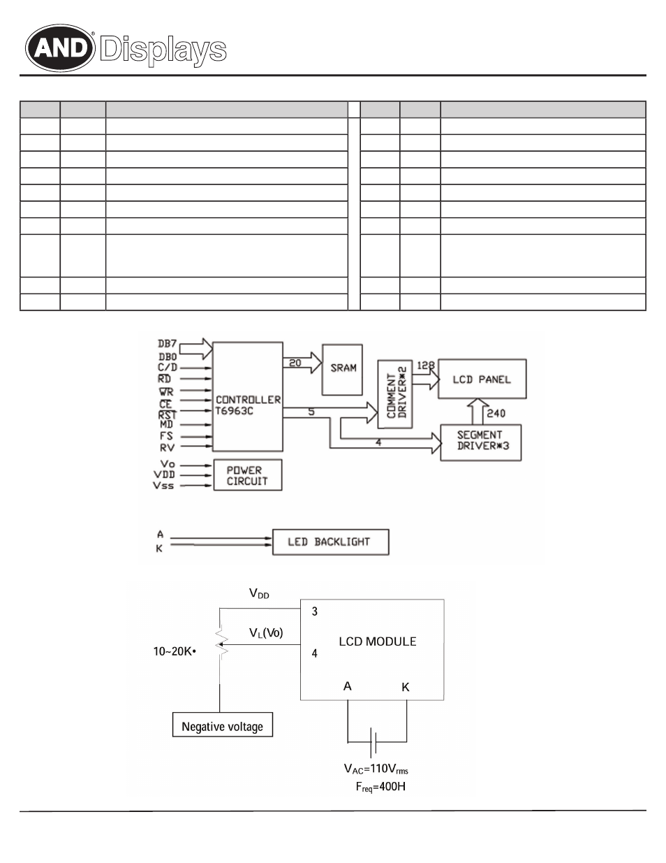
Block Diagram
AND1013ST-EO2
Intelligent Character Display
Power Supply