Avago Technologies ACNT-H313-000E User Manual
User's manual, Acnt-h313
ACNT-H313
Isolated IGBT/Power MOSFET Gate Driver Evaluation Board
User's Manual
Quick Start
Visual inspection is needed to ensure that the evaluation board is received in good condition.
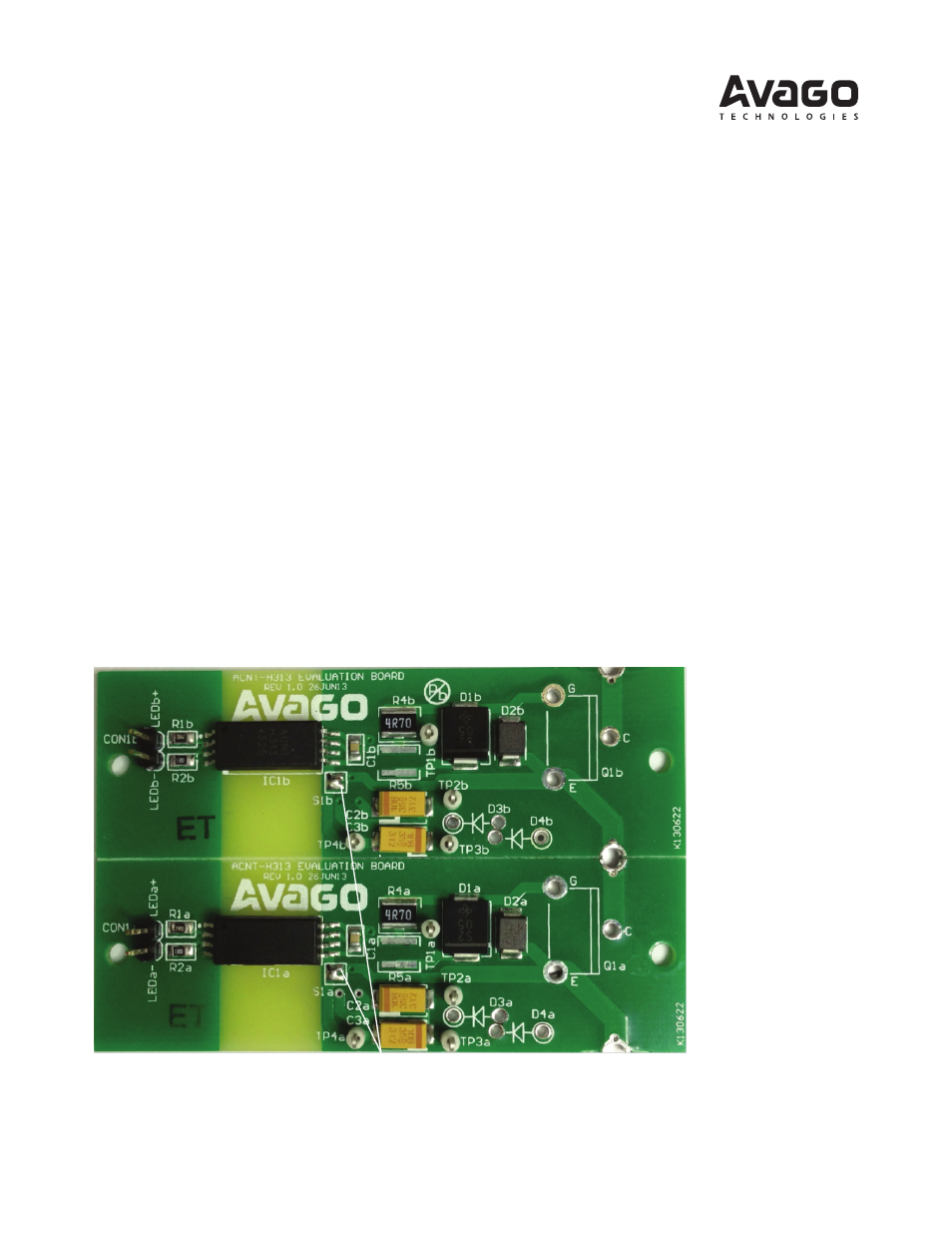
All part references are designated with the suffix ‘a’ and ‘b’ to indicate the lower and the upper inverter arm, respectively.
Default connections of the evaluation board are as shown in Figure 1:
1. Q1 not mounted. Actual switcher (IGBT or Power MOSFET) can be mounted at Q1 (in TO-247 package) or connected
to the driver board through short wire connections from the holes provided at Q1.
2. D5 and R7 are not mounted (on solder side). A 15 V Zener footprint at D5 can be inserted to allow for a single DC
power supply of 18 V~30 V to be applied across VCC2 and VEE if needed. A virtual ground VE (at Source pin Q1) can
then be generated and it acts as the reference point of each switcher. VCC2 will then stay at 15 V above the virtual
ground Ve. R7 is needed to generate the bias current across D5.
3. The S1 jumper is shorted by default to connect VE to VEE, assuming that a negative supply is not needed. Note: If a
negative supply is needed, then the S1 jumper needs to be removed;
4. Bootstrap diodes D3b and D4b are not connected by default. Insert these two components--together with R6a--to
generate the VCC2b supply through bootstrapping when the VCC2a supply is available. Note: Bootstrapping a supply
works only when Q1a and Q1b are mounted in a half-bridge configuration and are turned on and off through proper
PWM driving signals.
5. The S2 jumper is shorted by default; capacitance across VCC2 will be increased. When a negative supply for VEE is
needed, then the S2 jumper must be removed.
S2 on solder side (shorted)
S1 (shorted)
Bootstrapped linkage on solder side (soldered)
Figure 1. Actual ACNT-H313 evaluation board showing default connections
Once inspection is done, the evaluation board can be powered up in four simple steps, according to Figure 2 as shown,
to test either of the top and bottom half-bridge inverter arms in simulation mode without the need of an actual switcher.