Avago Technologies ACPL-P345-000E User Manual
User's manual, Isolated power mosfet gate driver evaluation board, Quick start
ACPL-P346/W346
Isolated Power MOSFET Gate Driver Evaluation Board
User's Manual
Quick Start
Visual inspection is needed to ensure that the evaluation board is received in good condition.
All part references are designated with suffix ‘a’ and ‘b’ to indicate the lower and the upper inverter arms, respectively. If
part references are made without suffixes, then they are valid for both upper and lower inverter arms (except R6, which
is shared).
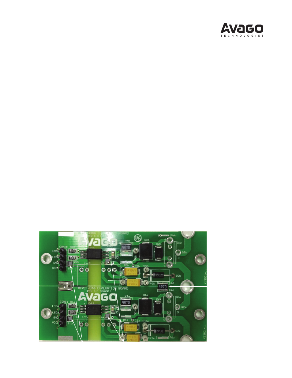
Figure 1 shows the default connections of the evaluation board:
1. Q1 and Q2 are not mounted. Actual Power MOSFET can be mounted at either Q1 (for TO-220 package) or Q2 (for TO-
247 package) or connected to the driver board through short wire connections from the holes provided at Q1 or Q2.
2. D4 and R7 are not mounted (on solder side). A 12 V Zener diode footprint at D4 is provided to allow for a single DC
power supply of 15 V ~25 V to be applied across V
CC2
and V
EE
if needed. A virtual ground V
E
(at Source pin of Q1 or
Q2) can then be generated and it acts as the reference point at the source pin of each power MOSFET. V
CC2
will then
stay at 12 V above the virtual ground V
E
. R7 is needed to generate the bias current across D4.
3. S2 and S3 jumpers are shorted by default to connect V
E
to V
EE
, assuming that a negative supply is not needed. Note:
If a negative supply is needed, then S2 and S3 jumpers must be removed.
4. Bootstrap diode D3b and resistor R6 are connected by default. These two components are provided to help generate
V
CC2b
supply through bootstrapping assuming that V
CC2a
supply is available. Note: Bootstrapping supply works
only when Q1 or Q2 are mounted in a half-bridge configuration and turned on and off through proper PWM driving
signals.
5. S1 is shorted by default to ground the IN- (or LED-, the cathode of LED) pin when V
CC1
is supplied. This short can be
removed if IN- cannot be grounded.
6. Upper and lower arms of the inverter will have common V
CC1
(and GND1), a provision is made to allow V
CC1
to be
connected by solder between upper and lower inverter PCB portions (and GND1 on the solder side).
7. Provisions are also made to allow V
CC2
(and V
EE
) to be generated from V
CC1
through a DC/DC converter at IC2. When
this DC/DC converter is used, S2, S3 (and R6) should be disconnected.
Figure 1. Actual ACPL-P346/W346 evaluation board showing default connections
VCC1a and VCC1b (shorted)
GNDa and GNDb on solder side (also shor
ted)
S1 (shorted)
S2 (shorted)
S3 on solder side (also shorted)
R6 moun
ted (shor
ted)
V
CC1b
V
CC1a