Altera Transceiver Signal Integrity Development Kit, Stratix IV GT Edition User Manual
Page 23
Chapter 2: Board Components
2–13
Configuration, Status, and Setup Elements
November 2011
Altera Corporation
Transceiver Signal Integrity Development Kit,
Stratix IV GT Edition Reference Manual
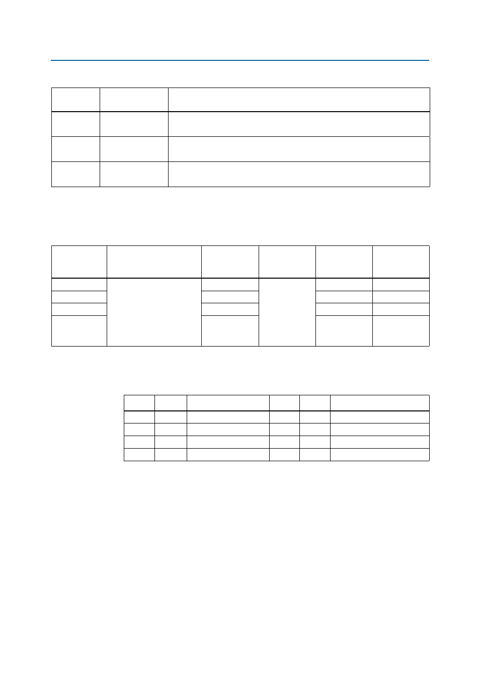
There is a spread spectrum configuration DIP switch (SW2) for configuring the spread
spectrum clock device (U21).
lists the connection of the spread spectrum
configuration DIP switch (SW2).
summarizes the functionality of the spread spectrum configuration DIP
switch (SW2).
J65
Y3 OSC
EN/DIS
When a jumper is installed, Y3 oscillator is disabled.
When a jumper is removed, Y3 oscillator is enabled and running.
J66
Y4 OSC
EN/DIS
When a jumper is installed, Y4 oscillator is disabled.
When a jumper is removed, Y4 oscillator is enabled and running.
J67
Y5 OSC
EN/DIS
When a jumper is installed, Y5 oscillator is disabled.
When a jumper is removed, Y5 oscillator is enabled and running.
Table 2–7. Board Jumpers (Part 2 of 2)
Board
Reference
Jumper Name
Description
Table 2–8. Spread Spectrum Configuration DIP Switch Pin-Out (SW2)
Board
Reference
Description
Schematic
Signal Name
I/O Standard
Stratix IV GT
Device
Pin Name
Other
Connections
SW2 pin 1 (S0)
Spread spectrum clock
configuration DIP switch.
When the switch is in the
open position, a logic 1 is
selected. When the switch is
in the closed position, a logic
0 is selected.
S0
2.5-V CMOS
—
U21 pin 1
SW2 pin 2 (S1)
S1
—
U21 pin 2
SW2 pin 3 (S2)
SS0
—
U21 pin 3
SW2 pin 4 (S3)
SS1
—
U21 pin 8
Table 2–9. Spread Spectrum Configuration DIP Switch (SW2) Configuration
S1
S0
Clock Frequency
S3
S2
Spread Spectrum %
0
0
25 MHz
0
0
Center ±25
0
1
100 MHz
0
1
Down –0.50
1
0
125 MHz
1
0
Down –0.75
1
1
200 MHz
1
1
No spread spectrum