Altera LCD Multimedia HSMC User Manual
Page 14

Altera Corporation
2–6
August 2008
LCD Multimedia HSMC
Board Components and Interfaces
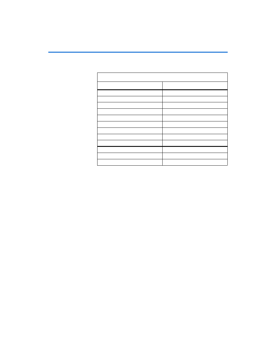
Table 2–4
lists the Max II EPM2210F324C4 device pin count.
f
For additional information about Altera devices, go to
.
Block Diagram of bus-controller logic in the MAX II CPLD
shows the block diagram of Bus Controller logic in the MAX
II device. Both the LCD TDM block is a simple 8-bit to 24-bit data
de-multiplexing function which drives the LCD panel. Similarly, the
VGA TDM block is a 10bit to 30bit data de-multiplexing function which
drives the VGA DAC. In the LCD TDM block, the 8-bit input data
(successive BGR color data) comes in at 3x the rate of the 24-bit output
data bus (8-bit B + 8bit G + 8bit R).
1
The purpose of adding this complexity to the design of the LCD
Multimedia HSMC was to allow for more functionality given
the constraint of a pin-limited HSMC connector interface.
The I2CBir_bus block provides birdirectional control for I2C Serial
EEPROM data bus. All other signals that pass through the MAXII device
are uni-directional and are simply buffered and level-shifted in the
MAX II.
Table 2–4. Max II Device Pin Count
Board Component
Pins
SD Card
6
Ethernet
18
Audio Codec
6
RS232 and PS/2
4
LCD Touch Panel
38
Video Decoder
14
VGA
25
MAX II CPLD ISP
4
HSMC(1)
88
Total Pins Used
203
Total EPM2210F324C4 User I/Os
272
Unused pins
69
Note to
Table 2–4
:
(1)
The HSMC pins include all pins between the FPGA and the MAX II CPLD