Chapter 2 - hardware installation, Board layout, Block diagram – DFI Q7X-151 User Manual
Page 7: Block diagram q7 connector, Sata 1x, Pcie x4 msata, Sm bus i
www.dfi .com
Chapter 2 Hardware Installation
7
Chapter 2
Chapter 2 - Hardware Installation
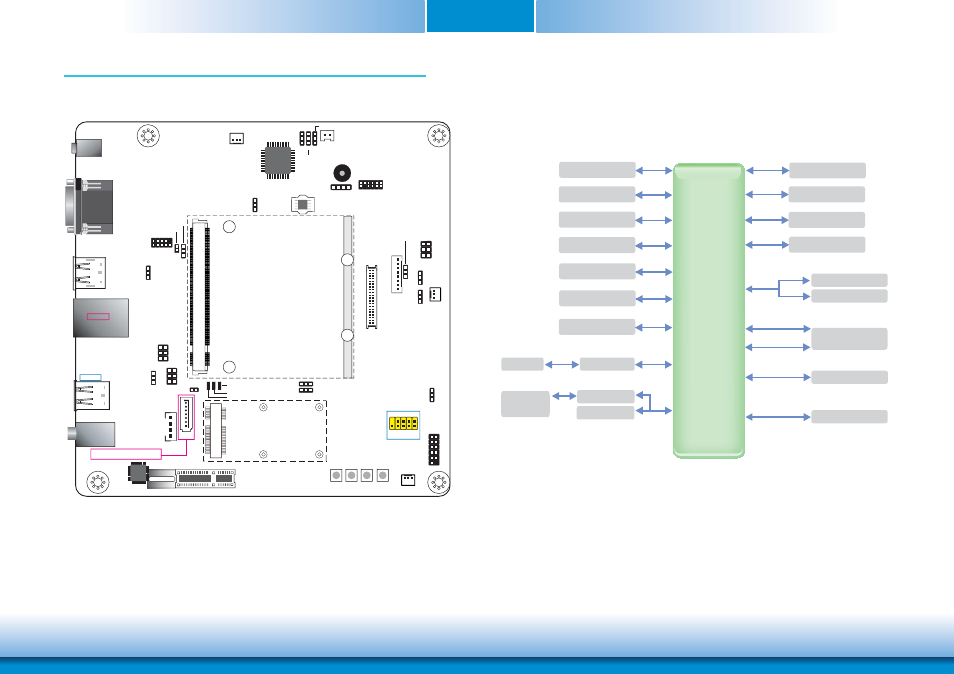
Board Layout
1
1
1
1
1
1
2
1
39
40
LVDS LCD
Panel
SPI Flash
BIOS
1
2
Battery
1
2
11
12
1 1 1
PCIe x4
1
1
11
12
2
2
1
10
9
1
1
1
COM 4
COM 3
LAN
USB 0-1
Line-in
Line-out
Mic-in
USB 3.0
USB 2-3
USB 2.0
2
1
6
5
UART 1
LCD/Inverter
Power
NUVOTON
NCT6106D
CAN Bus
LCD/Inverter
Power Select (JP17)
Backlight Power
Select (JP16)
USB 2.0
Note:
The SATA port supports SATA DOM.
MXM
UART 2
1
System Fan 1
1
System
Fan 2
1
System
Fan 3
Lid
Sleep Power Reset
USB 0-1 Power
Select (JP1)
USB 2-3 Power
Select (JP2)
Dimming Mode
Select (JP11)
UART 2 Enable/Disable (JP3)
SPI Switch (JP4)
USB 4-5 Power
Select (JP23)
BIOS
Select (J9)
LVDS Switch Setting - Channel B (JP5)
LVDS Switch Setting - Channel A (JP6)
1
1
1
1
Panel Power
Select (JP21)
Super I/O
Enable/Disable (JP7)
Auto Power-on
Select (JP8)
Clear CMOS Data (JP9)
Buzzer
1
LPC
mSATA
Front
Panel
USB 4-5
SATA
1
4
SATA
Power
1
2
10
9
1
2
5
6
SMBus
1
2
5
6
DisplayPort
SATA 3.0
DC-in
I
2
C
Realtek
ALC886
Thermal Trip LED
Low Power State LED
SDIO LED
Block Diagram
Q7
Connector
SATA 1x
SATA 3.0
PCIe x4
mSATA
USB 2.0 port 0-1
USB 2.0 port 2-5
SM Bus
I
2
C Bus
Serial Port
CAN Bus
Display Port
SLP & LID
SDIO
LPC
USB 3.0 port 0
GLAN
SPI ROM
SPI Header
USB 3.0 1x
USB 2.0 4x
LVDS
ALC886
Audio
LPC Bus
COM 2x
SIO Fan
Super I/O