Ordering information, Electrical specifications, Pin assignments – Linx Technologies EVM-GPS-F4 User Manual
Page 4: Pin descriptions
– –
– –
2
3
Ordering Information
Ordering Information
Part Number
Description
EVM-GPS-F4
F4 Series Evaluation Module
RXM-GPS-F4
F4 Series GPS Receiver Module
Figure 2: Ordering Information
Electrical Specifications
Ordering Information
Parameter
Designation Min. Typ. Max. Units
Notes
POWER SUPPLY
Supply Voltage
V
CC
1.71
1.8
1.89
VDC
Input Pin Voltage
3.6
VDC
Output Pin Voltage
1.8
VDC
Supply Current
I
CC
Peak
130
mA
1
Acquisition
46
mA
1
Tracking
27.5
mA
1
Hibernate
20
µA
2
Ready-to-Start
9
µA
2
ANTENNA PORT
RF Input Impedance
R
IN
50
Ω
ENVIRONMENTAL
Operating Temperature Range
–30
+85
°C
Storage Temperature Range
–40
+85
°C
Figure 3: Electrical Specifications
Notes:
1. V
CC
= 1.8V
2. Initial state after power us applied
Warning:
This product incorporates numerous static-sensitive
components. Always wear an ESD wrist strap and observe proper ESD
handling procedures when working with this device. Failure to observe
this precaution may result in module damage or failure.
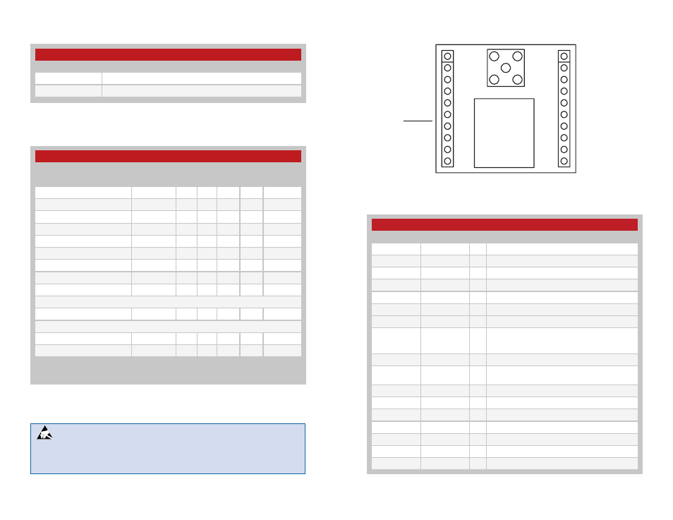
Pin Assignments
GND
NC
NC
VCC
NC
VBACKUP
GPIOC
GPIOB
GPIOA
GND
GND
GPIOD
GPIOE
TXM
RXM
1PPS
RESET
RFPWRUP
ON_OFF
GND
Figure 4: EVM-GPS-F4 Pin Assignments
Pin Descriptions
Pin Descriptions
Pin Number
Name
I/O Description
1
GPIOD
I/O General Purpose I/O. 3.6V tolerant.
2
GPIOE
I/O General Purpose I/O. 3.6V tolerant.
3
1PPS
O
1 Pulse Per Second. 1.8V level.
4
TX
O
Serial output (default NMEA)
5
RX
I
Serial input (default NMEA). 3.6V tolerant.
6
GPIOC
I/O General Purpose I/O. 3.6V tolerant.
7, 11
P1, P2
I
Pull to 1.8V VCC through 2.2k resistors.
8
/RESET
I
Reset Input. Active low with an internal pull-up.
Internal reset is preferred; external reset will clear all
RAM. 3.6V tolerant.
9
RFPWRUP
O
Power State Indicator
10
ON_OFF
I
Power Control Pin. Internal 10k pull-down resistor.
3.6V tolerant.
12
VCC
P
Supply Voltage
13
G1
I
Pull to GND through a 100k resistor.
14
GPIOA
I/O General Purpose I/O. 3.6V tolerant.
15
GPIOB
I/O General Purpose I/O. 3.6V tolerant.
16, 17
NC
−
No electrical connection.
18, 20, 21, 22
GND
P
Ground
19
RFIN
I
GPS RF signal input
Figure 5: F4 Series GPS Receiver Pin Descriptions