Schematic, Pcb layout, Power supply requirements – Linx Technologies EVM-GPS-F4 User Manual
Page 5: Schematic power supply requirements
– –
– –
4
5
GND
TX
M
TX_SHIFT
VCC
NC
1
IN
2
GND
3
OU
T
4
VCC
5
U4
MC74VHC1GT5
0
GND
RX
M
RX_SHIFT
V1.8
NC
1
IN
2
GND
3
OU
T
4
VCC
5
U5
MC74VHC1GT5
0
GP0/D
1
GND
2
GP1/C
3
GP
2
4
VCC
5
GP3/P
6
U2
VCC
ON_OFF
GND
GND
R6 100K
VPP
RFPWRUP
D1
PGD
PGC
R5
100
K
V1.8
R1
0
VPRG
VCC
GND
GND
GND
VBACKUP
C3 1uF
C2 1uF
V1.8
Vi
n
1
GND
3
Vout
2
U3
VCC
A
1
NC
2
D
C
G
5
S
6
3,8
4,
7
U6
FDFMA2P857
ON_OFF
TX
M
RX
M
VCC
GND
GND
GND
GND
GND
GND
GPIO
A
GPIO
B
GPIO
C
1PPS
RFPWRUP
GPIO
D
GPIO
E
C1
18pF
R4
2.2
K
R3
100K
R2
2.2
K
GPIO
D
1
GPIO
E
2
1PPS
3
TX
4
RX
5
GPIO
C
6
P1
7
/RESET
8
RFPWRUP
9
ON_OFF
10
P2
11
VCC
12
G1
13
GPIO
A
14
GPIO
B
15
NC
16
NC
17
GND
18
RFI
N
19
GND
20
GND
21
GND
22
U1
RXM-GPS-F
4
RF
1
GND
2-5
ANT1
CONSMA00
1
GND
L1 300ohm
BEAD
V1.8
V1.8
/RESET
GND
PGC
PGD
VPP
MCL
R
1
VDD
2
GND
3
PGD
4
PGC
5
NC
6
J3
Program
Header
VPRG
1 2 3 4 5 6 7 8 9 10
J1
1 2 3 4 5 6 7 8 9 10
J2
GND
GND
GND
GND
TX_SHIFT RX_SHIFT
1PP
S
RFPWRUP
GPIOC GPIOB GPIOA
GPIOD GPIOE
ON_OFF
VCC
/RESET
VBACKUP
/RESE
T
Schematic
Power Supply Requirements
The transceiver incorporates a precision
low-dropout regulator which allows operation
over a wide input voltage range. Despite this
regulator, it is still important to provide a supply
that is free of noise. Power supply noise can
significantly affect the module’s performance, so
providing a clean power supply for the module
should be a high priority during design.
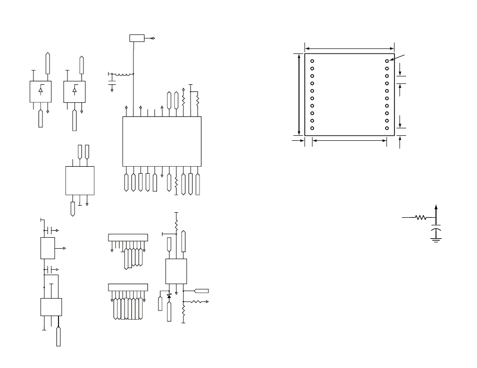
A 10
Ω resistor in series with the supply followed by a 10µF tantalum
capacitor from V
cc
to ground helps in cases where the quality of supply
power is poor (Figure 7). This filter should be placed close to the module’s
supply lines. These values may need to be adjusted depending on the
noise present on the supply line.
+
10
Ω
10
µF
Vcc IN
Vcc TO
MODULE
Figure 7: Supply Filter
1.20”
(47.24)
0.10”
(2.54)
0.10”
(2.54)
0.10”
(2.54)
1.10”
(27.94)
1.00”
(25.40)
Ø0.04” x 10
(1.02)
PCB Layout
Figure 6: EVM-GPS-F4 PCB Layout Dimensions