Theory of operation, Power-up sequence, Power supply – Linx Technologies RXM-900-HP3-xxx User Manual
Page 4: Using the pdn pin
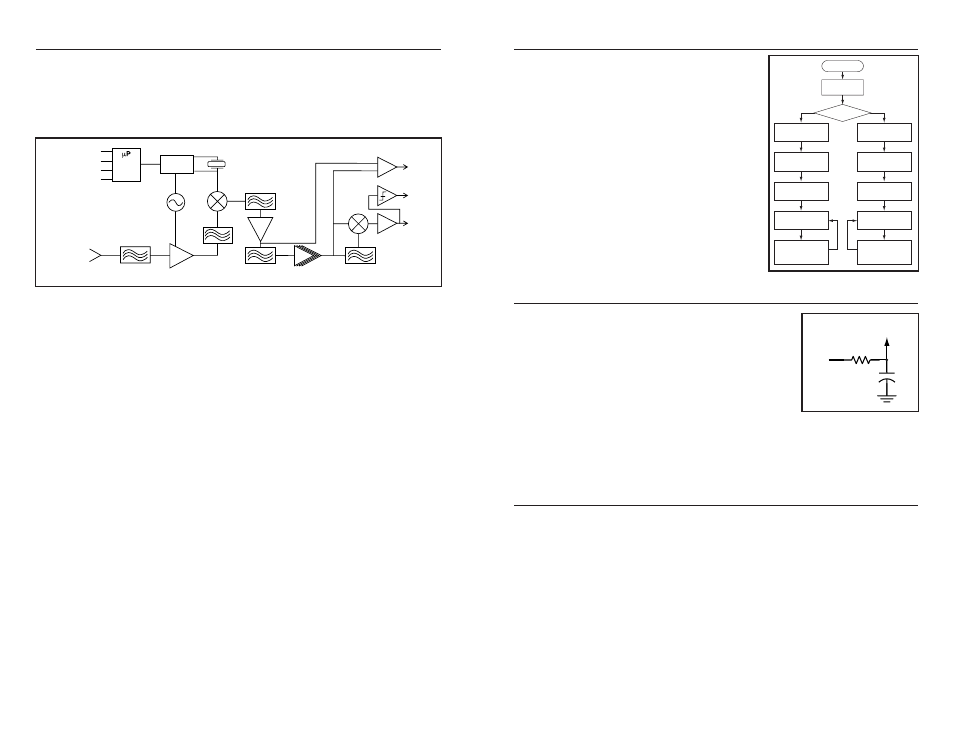
THEORY OF OPERATION
The HP3 is a high-performance multi-channel, dual-conversion superhet
receiver capable of recovering both analog (FM) and digital (FSK) information
from a matching HP Series transmitter. FM / FSK modulation offers significant
advantages over AM or OOK modulation methods, including increased noise
immunity and the receiver’s ability to capture in the presence of multiple signals.
This is especially helpful in crowded bands, like that in which the HP3 operates.
The single-ended RF port is matched to 50-ohms to support commonly available
antennas, such as those manufactured by Linx. The RF signal coming in from
the antenna is filtered by a Surface Acoustic Wave (SAW) filter to attenuate
unwanted RF energy. A SAW filter provides significantly higher performance
than other filter types, such as an LC bandpass filter.
Once filtered, the signal is amplified by a Low Noise Amplifier (LNA) to increase
the receiver sensitivity and lower the overall noise figure of the receiver. After the
LNA, the signal is mixed with a synthesized local oscillator operating 34.7MHz
below the incoming transmission frequency to produce the first Intermediate
Frequency (IF).
The second conversion and FM demodulation is achieved by a high-
performance IF strip that mixes the 34.7MHz first conversion frequency with
24.0MHz from a precision crystal oscillator. The resulting second IF of 10.7MHz
is then highly amplified in preparation for demodulation.
A quadrature demodulator is used to recover the baseband signal from the
carrier. The demodulated waveform is filtered, after which it closely resembles
the original signal. The signal is routed to the analog output pin and the data
slicer stage, which provides squared digital output via the data output pin. A key
feature of the HP3 is the transparency of its digital output, which does not impose
balancing or duty-cycle requirements within a range of 100bps to 56kbps.
An on-board microcontroller manages receiver functions and greatly simplifies
user interface. The microcontroller reads the channel selection lines and
programs the on-board synthesizer. This frees the designer from complex
programming requirements and allows for manual or software channel selection.
The microcontroller also monitors incoming signal strength and squelches the
data output when the signal is not strong enough for accurate data detection.
Page 7
Page 6
Channel
Select
SAW BPF
VCO
PLL
{
4MHz
Int. Osc.
MODE
CS0
CS1
CS2
LNA
34.7M
BPF
10.7MHz
BPF
24MHz
Crystal
IF
Amp
10.7M
BPF
10.7M
Discriminator
Quad
RSSI
Digital
Data
Analog
Data
Limiter
Figure 9: HP3 Series Receiver Block Diagram
POWER-UP SEQUENCE
As previously mentioned, the HP3 is controlled
by an on-board microprocessor. When power
is applied, the microprocessor executes the
receiver start-up sequence, after which the
receiver is ready to receive valid data.
The adjacent figure shows the start-up
sequence. This sequence is executed when
power is applied to the V
CC
line or when the
PDN line is taken high.
On power-up, the microprocessor reads the
external channel selection lines and sets the
frequency synthesizer to the appropriate
channel. Once the frequency synthesizer has
stabilized, the receiver is ready to accept data.
POWER SUPPLY
The HP3 incorporates a precision, low-dropout
regulator on-board, which allows operation over an
input voltage range of 2.8 to 13 volts DC. Despite this
regulator, it is still important to provide a supply that
is free of noise. Power supply noise can significantly
affect the receiver sensitivity; therefore, providing a
clean power supply for the module should be a high
priority during design.
A 10
Ω resistor in series with the supply followed by a
10µF tantalum capacitor from V
CC
to ground will help in cases where the quality
of supply power is poor. This filter should be placed close to the module’s supply
lines. These values may need to be adjusted depending on the noise present on
the supply line.
USING THE PDN PIN
The Power Down (PDN) line can be used to power down the receiver without the
need for an external switch. This line has an internal pull-up, so when it is held
high or simply left floating, the module will be active.
When the PDN line is pulled to ground, the receiver will enter into a low-current
(<10µA) power-down mode. During this time the receiver is off and cannot
perform any function. It may be useful to note that the startup time coming out
of power-down will be slightly less than when applying V
CC
.
The PDN line allows easy control of the receiver state from external
components, like a microcontroller. By periodically activating the receiver,
checking for data, then powering down, the receiver’s average current
consumption can be greatly reduced, saving power in battery-operated
applications.
POWER ON
Squelch Data
Output Pin
Determine Mode
Program Freq. Synth
To Default CH. 50
Read Channel
Selection Inputs
Crystal Oscillator
Begins to Operate
Program Frequency
Synthesizer
Ready for
Serial Data Input
Crystal Oscillator
Begins to Work
Determine Squelch
State Data Output Pin
Cycle Here Until More
Data Input
or Mode Change
Determine Squelch
State Data Output Pin
Cycle Here Until
Channel
or Mode Change
Serial Mode
Parallel Mode
Figure 10: Start-Up Sequence
+
10
Ω
10
μF
Vcc IN
Vcc TO
MODULE
Figure 11: Supply Filter