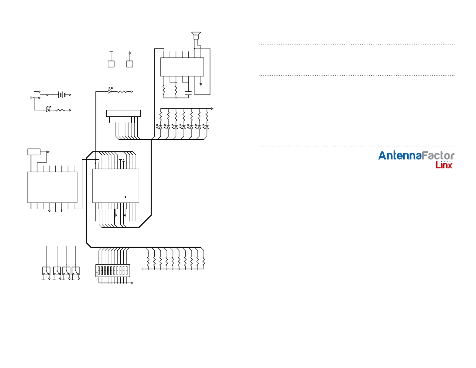
Ds series decoder evaluation board schematic, Resources, Figure 7: ds series decoder board schematic – Linx Technologies OEM Transmitter Evaluation Kit User Manual
Page 8
–
–
–
–
10
11
Resources
Support
For technical support, product documentation, application notes, regulatory
guidelines and software updates, visit www.linxtechnologies.com
RF Design Services
For customers who need help implementing Linx modules, Linx offers
design services including board layout assistance, programming,
certification advice and packaging design. For more complex RF solutions,
Apex Wireless, a division of Linx Technologies, creates optimized designs
with RF components and firmware selected for the customer’s application.
Call +1 800 736 6677 (+1 541 471 6256 if outside the United States) for
more information.
Antenna Factor Antennas
Linx’s Antenna Factor division has the
industry’s broadest selection of antennas
for a wide variety of applications. For
customers with specialized needs, custom
antennas and design services are available along with simulations of
antenna performance to speed development. Learn more at
www.linxtechnologies.com.
by
D1
R6
200
D2
R9
200
D3
R11
200
D4
R15
200
D5
R17
200
D6
R19
200
D7
R20
200
D0
D1
D2
D3
D4
D5
D6
D7
GND
1 2 3
20 19 18
4 5 6
17 16 15
7 8 9
14 13 12
10
11
S1
GND
A0 A1 A2 A3 A4 A5 A6 A7 A8 A9
GND
BZ1
B`
4
C
5
C`
6
GND
7
B
3
A`
2
A
1
E
11
F`
12
F
13
VCC
14
E`
10
D
9
D`
8
U3
C1
0.01u
F
R7
100k
R1
2
10
k
A[0..9
]
D[0..7]
E/D_SE
L
A_CFG0 A_CFG1
TE/DIN
DOUT/VT
P_SE
L
D0 D1 D2 D3 D4 D5 GND D6 D7
D_CF
G
1 2 3 4 5 6 7 8 9 10 11 12 13 14
A0
A1
A2
A3
GND
VCC
A4
A5
A6
A7
A8
A9
15
16
17
18
19
20
21
22
23
24
25
26
27
28
U2
LICAL-EDC-DS001
D0 D1 D2 D3 D4 D5
D6 D7
GND
GND
A0
A1
A2
A3
A4
A5
A6
A7
A8
A9
GND
VCC
P_SE
L
D_CF
G
A_CFG0 A_CFG1
VCC
R4
R5
R8
R10
R13
R14
R16
R18
R3
R2
100k
100k
100k
100k
100k
100k
100k
100k
100k
100k
A0
A1
A2
A3
A4
A5
A6
A7
A8
A9
SW2
SW3
SW4
SW1
VCC
VCC
VCC
GND
GND
GND
VCC
GND
P_SEL
D_CF
G
A_CFG0
A_CFG1
ANT1
GND
GND
VCC
NC
1
NC
2
NC
3
GND
4
VCC
5
PDN
6
RSSI
7
DATA
8
NC
9
NC
10
NC
11
NC
12
NC
13
NC
14
GND
15
ANT
16
U1
RXM-XXX-LR
RF
1
GND
2-5
CONREVSMA001
VCC
DIN
D0 D1 D2 D3 D4 D5 D6 D7
DIN VT
1 2 3 4 5 6 7 8 9 10
J1
HEADER
10
1
TP
1
1
TP
2
VCC
GND
GND
VCC
S2
B1 BAT-HLD-AA
A
GND
R21 620
ohm
D8
POWER GREEN
D9
R1 200
ohm
GND
VT
VALID TXM BLUE
Figure 7: DS Series Decoder Board Schematic
DS Series Decoder Evaluation Board Schematic