7 specifications, performance, 1 voltage control channel, Specifications, performance -3 – KEPCO JQE 150-1.5MVPY-26956 Half Rack User Manual
Page 13: Voltage control channel -3, E 1-2 list
JQE 26956 081111
1-3
1.7
SPECIFICATIONS, PERFORMANCE
1.7.1
VOLTAGE CONTROL CHANNEL
a) LOCAL OUTPUT VOLTAGE CONTROL: 10-turn precision potentiometer at the front
panel, resolution: 0.1% of the maximum rated output voltage (E
O
max.). When the E
OUT
LOC-REM switch (accessible through the top cover) is set to LOC (towards the front
panel), this pot controls output voltage from zero to E
O
max. Both ZERO and FS (full
scale) calibrations are provided. Local voltage control from the front panel is enabled by
the link installed on the rear panel terminal block TB501, between terminals 6 (RVC) and
7 (RPV1); the remote voltage control resistor between terminals 7 (RPV1) and 8 (RPV2)
must be removed.
b) REMOTE OUTPUT VOLTAGE CONTROL: When the E
OUT
LOC-REM switch (accessi-
ble through the top cover) is set to REM (towards the rear panel), external control can be
exercised by resistance (1000 ohms per volt of output); refer to Section 3 for details. This
allows the output to be controlled from zero to E
O
max with an accuracy of 0.1% of E
O
nominal. Both ZERO (same as LOCAL ZERO) and FS (full scale) calibrations are pro-
vided. Remote voltage control using resistance is enabled by removing the link installed
on the rear panel terminal block TB501 between terminals 6 (RVC) and 7 (RPV1) and
installing the voltage control resistor between terminals 7 (RPV1) and 8 (RPV2).
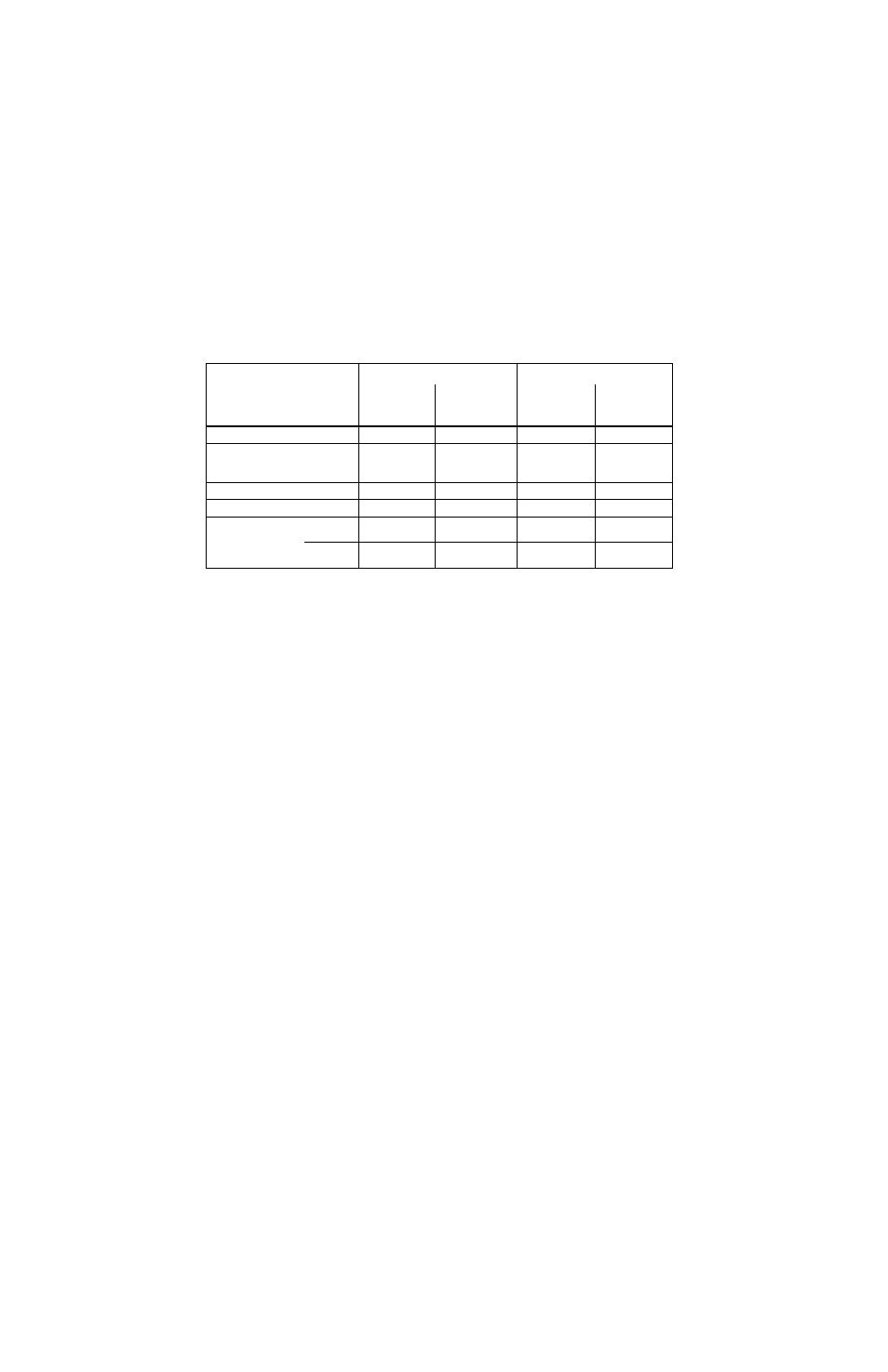
TABLE 1-2. JQE SPECIAL MODELS, COMMON ELECTRICAL SPECIFICATIONS
INFLUENCE QUANTITY
OUTPUT EFFECTS
AMPLIFIER OFFSETS(3)
VOLTAGE
MODE
∆
E
O
CURRENT MODE
∆
I
O
(2)
VOLTAGE MODE
∆
E
O
CURRENT MODE
∆
I
O
Source effect: 105-125/210-250V a-c
<0.0005%
<0.005%
<10
µ
V
<2nA
Load effect: no load - full load
for voltage mode: full load
for current limit mode: short-circuit
<0.005% or
0.2mV (1)
3mA
<200
µ
V
<5nA
Time effect: 8 hours (drift)
<0.01% or 1mV
< 0.1%
<20
µ
V
<2nA
Temperature effect: per °C
<0.01%
<0.1%
<20
µ
V
<5nA
Ripple and Noise(4)
Ripple
<0.2mV
<0.02% of
I
O
max
-
-
Noise
<1.0mV
<0.1% of
I
O
max
(1) Whichever is greater.
(2) Current Mode Output Effects (
∆
I
O
) are measured across an external sensing resistor. This resistor must be a high
quality, wirewound unit, with a wattage at least 10 times the actual power dissipated, have a Temperature Coeffi-
cient of 20 parts per million or better, include adequate cooling, and drop a sample voltage of 1.0 Volt at the mea-
suring current. A resistor built as a 4-terminal network is recommended. Current feedback is exercised with an
internal 20 PPM feedback resistor.
(3) Offsets and the reference contribute t o output effect
∆
E
O
, by the equation
∆
E
O
=
∆
E
ref
(R
f
/ R
i
)
±∆
E
io
(1 + R
f
/ R
i
) (R
f
)
where R
f
is the feedback resistor and R
i
is the input resistor from the signal reference. Use the offsets t o calculate
output effects when external input/feedback elements are substituted for the internal reference and voltage con-
trol in special applications.
(4) Valid with one output terminal grounded or connected so that the common mode current (see PAR. 1.5e) does not
flow through the load or (in current mode) through a sensing resistor. Evaluated in the 20Hz to 10MHz frequency
range.