Dflz5v1q - dflz39q, Maximum ratings, Thermal characteristics – Diodes DFLZ5V1Q - DFLZ39Q User Manual
Page 2: Electrical characteristics
DFLZ5V1Q - DFLZ39Q
Document number: DS36898 Rev. 1 - 2
2 of 4
February 2014
© Diodes Incorporated
DFLZ5V1Q - DFLZ39Q
POWERDI is a registered trademark of Diodes Incorporated.
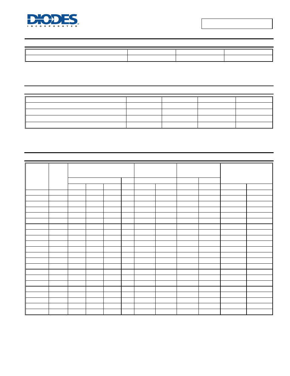
Maximum Ratings
(@T
A
= +25°C, unless otherwise specified.)
Characteristic Symbol
Value
Unit
Forward Voltage
@ I
F
= 200mA
V
F
1.2 V
Thermal Characteristics
Characteristic Symbol
Typ
Value
Unit
Power Dissipation (Note 5)
P
D
— 1.0 W
Thermal Resistance Junction to Ambient Air (Note 5)
R
θJA
110 —
°C/W
Thermal Resistance Junction to Soldering Point (Note 6)
R
θJS
— 9
°C/W
Operating and Storage Temperature Range
T
J
, T
STG
—
-55 to +150
°C
Electrical Characteristics
(@T
A
= +25°C, unless otherwise specified.)
Type
Number
Marking
Codes
Zener Voltage Range
(Note 7)
Zener Impedance
(Note 8)
Maximum Reverse
Current
(Note 7)
Temperature
Coefficient
@ I
ZTC
%/
°C
V
Z
@ I
ZT
I
ZT
Z
ZT
@
I
ZT
I
R
@
V
R
Nom (V) Min (V) Max (V)
mA
Typ
(Ω) Max
(
Ω)
μA
V Min Max
DFLZ5V1Q
FHK 5.1 4.8 5.4
100 2
6
2.5
1
-0.08
-0.2
DFLZ5V6Q
FHL 5.6 5.2 6.0
100 1
4
10
2
-0.04
0.04
DFLZ6V2Q
FHN 6.2 5.8 6.6
100 1
3
5
2
-0.01
0.06
DFLZ6V8Q
FHO 6.8 6.4 7.2
100 1
3
5
3
0
0.07
DFLZ7V5Q
FHQ 7.5 7.0 7.9
100 1
2
5
3
0
0.07
DFLZ8V2Q
FHR 8.2 7.7 8.7
100 1
2
5
3
0.03
0.08
DFLZ9V1Q
FHT 9.1 8.5 9.6 50 1
4
5
5
0.03
0.08
DFLZ10Q FHU 10 9.4 10.6 50 1
4
5
7.5
0.05
0.09
DFLZ11Q FHV 11 10.4 11.6
50 1
7
4
8.2
0.05
0.10
DFLZ12Q FHW 12 11.4 12.7 50 1
7
3
9.1
0.05
0.10
DFLZ13Q
FHX
13
12.4
14.1
50
1 10 2 10 0.05 0.10
DFLZ15Q
FHZ
15
13.8
15.6
50
1 10 1 11 0.05 0.10
DFLZ16Q
FJA
16
15.3
17.1
25
1 15 1 12 0.06 0.11
DFLZ18Q
FJF
18
16.8
19.1
25
2 15 1 13 0.06 0.11
DFLZ20Q
FJG
20
18.8
21.2
25
3 15 1 15 0.06 0.11
DFLZ22Q
FJK
22
20.8
23.3
25
3 15 1 16 0.06 0.11
DFLZ24Q
FJL
24
22.8
25.6
25
2 15 1 18 0.06 0.11
DFLZ27Q
FJN
27
25.1
28.9
25
3 15 1 20 0.06 0.11
DFLZ30Q FJQ 30 28 32
25 8
15
1
22
0.06
0.11
DFLZ33Q FJR 33 31 35
25 5
15
1
24
0.06
0.11
DFLZ36Q FJS 36 34 38
10 5
40
1
27
0.06
0.11
DFLZ39Q FJT 39 37 41
10 5
40
1
30
0.06
0.11
Notes:
5. Device mounted on 1" x 1", FR-4 PCB; 2 oz. Cu pad layout as shown on Diodes Inc. suggested pad layout document AP02001.pdf at
6 Theoretical R
θJS
calculated from the top center of the die straight down to the PCB/cathode tab solder junction.
7. Short duration pulse test used to minimize self-heating effect.
8. The Zener impedance (Zzt) is measured by superimposing a minute alternating current on the regulated current (Izt).