Djt4031n new prod uc t, Electrical characteristics, Djt4031n – Diodes DJT4031N User Manual
Page 2
DJT4031N
Document number: DS31603 Rev. 2 - 2
2 of 5
March 2009
© Diodes Incorporated
DJT4031N
NEW PROD
UC
T
Electrical Characteristics
@T
A
= 25°C unless otherwise specified
Characteristic Symbol
Min
Typ
Max
Unit
Test
Conditions
OFF CHARACTERISTICS (Note 4)
Collector-Base Breakdown Voltage
V
(BR)CBO
40
⎯
⎯
V
I
C
= 100
μA
Collector-Emitter Breakdown Voltage
V
(BR)CEO
40
⎯
⎯
V
I
C
= 10mA
Emitter-Base Breakdown Voltage
V
(BR)EBO
6
⎯
⎯
V
I
E
= 50
μA
Collector-Base Cutoff Current
I
CBO
⎯
⎯
100
nA
V
CB
= 40V, I
E
= 0
⎯
⎯
50
μA
V
CB
= 40V, I
E
= 0, T
A
= 150°C
Emitter-Base Cutoff Current
I
EBO
⎯
⎯
100 nA
V
EB
= 6V, I
C
= 0
ON CHARACTERISTICS (Note 4)
DC Current Gain
h
FE
220
⎯
⎯
⎯
V
CE
= 1V, I
C
= 0.5A
200
⎯
500
V
CE
= 1V, I
C
= 1A
100
⎯
⎯
V
CE
= 1V, I
C
= 3A
Collector-Emitter Saturation Voltage
V
CE(SAT)
⎯
⎯
100
mV
I
C
= 0.5A, I
B
= 5mA
⎯
⎯
150
I
C
= 1A, I
B
= 10mA
⎯
⎯
300
I
C
= 3A, I
B
= 0.3A
Equivalent On-Resistance
R
CE(SAT)
⎯
⎯
100
m
Ω I
E
= 3A, I
B
= 0.3A
Base-Emitter Saturation Voltage
V
BE(SAT)
⎯
⎯
1.0 V
I
C
= 1A, I
B
= 0.1A
Base-Emitter Turn-on Voltage
V
BE(ON)
⎯
⎯
1.0 V
V
CE
= 2V, I
C
= 1A
SMALL SIGNAL CHARACTERISTICS
Transition Frequency
f
T
⎯
105
⎯
MHz
V
CE
= 10V, I
C
= 100mA,
f = 100MHz
Output Capacitance
C
obo
⎯
27
⎯
pF
V
CB
= 10V, f = 1MHz
Input Capacitance
C
Ibo
⎯
180
⎯
pF
V
CB
= 5V, f = 1MHz
SWITCHING CHARACTERISTICS
Turn-On Time
t
on
⎯
45
⎯
ns
V
CC
= 10V, I
C
= 2A,
I
B1
= 200mA
Delay Time
t
d
⎯
14
⎯
ns
Rise Time
t
r
⎯
31
⎯
ns
Turn-Off Time
t
off
⎯
276
⎯
ns
V
CC
= 10V, I
C
= 2A,
I
B1
= I
B2
= 200mA
Storage Time
t
s
⎯
244
⎯
ns
Fall Time
t
f
⎯
32
⎯
ns
Notes:
4. Measured under pulsed conditions. Pulse width = 300
μs. Duty cycle ≤2%.
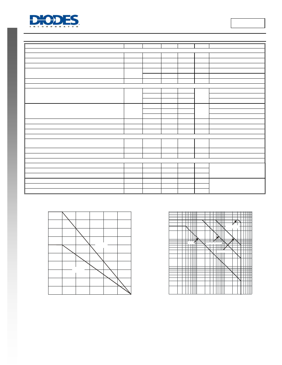
0
0
P
, P
OW
E
R
DI
S
S
IP
A
T
ION
(W
)
D
T , AMBIENT TEMPERATURE ( C)
A
°
(Note 3)
Fig. 1 Power Dissipation vs. Ambient Temperature
25
50
75
100
125
150
0.4
0.8
1.2
2.0
(Note 4)
1.6
0.01
0.10
1
10
0.1
1
10
100
V
, COLLECTOR-EMITTER VOLTAGE (V)
CE
Fig. 2 Typical Collector Current
vs. Collector-Emitter Voltage (Note 3)
I,
C
O
LL
E
C
T
O
R
C
U
R
R
E
N
T
(A
)
C
Pw = 100ms
Pw = 10ms
Pw = 1ms
DC