Maximum ratings, Thermal characteristics, Electrical characteristics – Diodes DMN3115UDM User Manual
Page 2: Dmn3115udm
DMN3115UDM
Document number: DS31187 Rev. 8 - 2
2 of 5
November 2013
© Diodes Incorporated
DMN3115UDM
Maximum Ratings
(@T
A
= +25°C, unless otherwise specified.)
Characteristic Symbol
Value
Units
Drain-Source Voltage
V
DSS
30 V
Gate-Source Voltage
V
GSS
±8 V
Drain Current (Note 6)
I
D
3.2 A
Pulsed Drain Current (Note 6)
I
DM
12.8 A
Thermal Characteristics
Characteristic Symbol
Value
Units
Total Power Dissipation (Note 6)
P
D
900 mW
Thermal Resistance, Junction to Ambient
R
θJA
139 °C/W
Operating and Storage Temperature Range
T
J
, T
STG
-55 to +150
°C
Electrical Characteristics
(@T
A
= +25°C, unless otherwise specified.)
Characteristic Symbol
Min
Typ
Max
Unit
Test
Condition
OFF CHARACTERISTICS (Note 7)
Drain-Source Breakdown Voltage
BV
DSS
30
V
V
GS
= 0V, I
D
= 100μA
Zero Gate Voltage Drain Current
I
DSS
1
μA V
DS
= 30V, V
GS
= 0V
Gate-Source Leakage
I
GSS
5
μA V
GS
=
8V, V
DS
= 0V
ON CHARACTERISTICS (Note 7)
Gate Threshold Voltage
V
GS(th)
0.5
1.0 V
V
DS
= V
GS
, I
D
= 250μA
Static Drain-Source On-Resistance
R
DS (ON)
40
50
76
60
80
130
mΩ
V
GS
= 4.5V, I
D
= 6A
V
GS
= 2.5V, I
D
= 2A
V
GS
= 1.5V, I
D
= 1.0A
Forward Transfer Admittance
|Y
fs
|
8
S
V
DS
=10V, I
D
= 6A
Diode Forward Voltage (Note 7)
V
SD
0.7 1.1 V V
GS
= 0V, I
S
= 2A
DYNAMIC CHARACTERISTICS
Input Capacitance
C
iss
476
pF
V
DS
= 15V, V
GS
= 0V
f = 1.0MHz
Output Capacitance
C
oss
77
pF
Reverse Transfer Capacitance
C
rss
59
pF
Notes:
6. Device mounted on FR-4 PCB, minimum recommended pad layout on 2oz. Copper pads.
7. Short duration pulse test used to minimize self-heating effect.
0
1
2
3
4
5
6
7
8
9
10
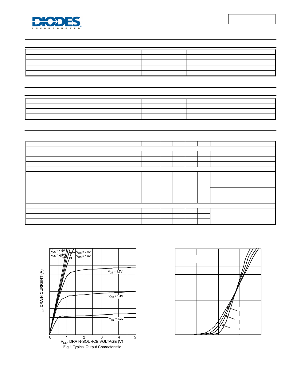
Fig. 2 Typical Transfer Characteristics
V , GATE SOURCE VOLTAGE (V)
GS
I,
D
R
AI
N
C
U
R
R
E
N
T
(A
)
D
T = -55°C
A
T = 25°C
A
T = 85°C
A
T = 150°C
A
V
= 5V
Pulsed
DS
0
1
2
3
4
5
6
7
8
9
10
0.5
1
1.5
2
0