Typical characteristics, Test circuits, Drain - source voltage (v) – Diodes DMP4050SSD User Manual
Page 6: Dmp4050ssd, A product line of diodes incorporated
Advertising
DMP4050SSD
Document Number DS32107 Rev 3 - 2
6 of 8
April 2013
© Diodes Incorporated
ADVAN
CE I
N
F
O
RM
ATI
O
N
A Product Line of
Diodes Incorporated
DMP4050SSD
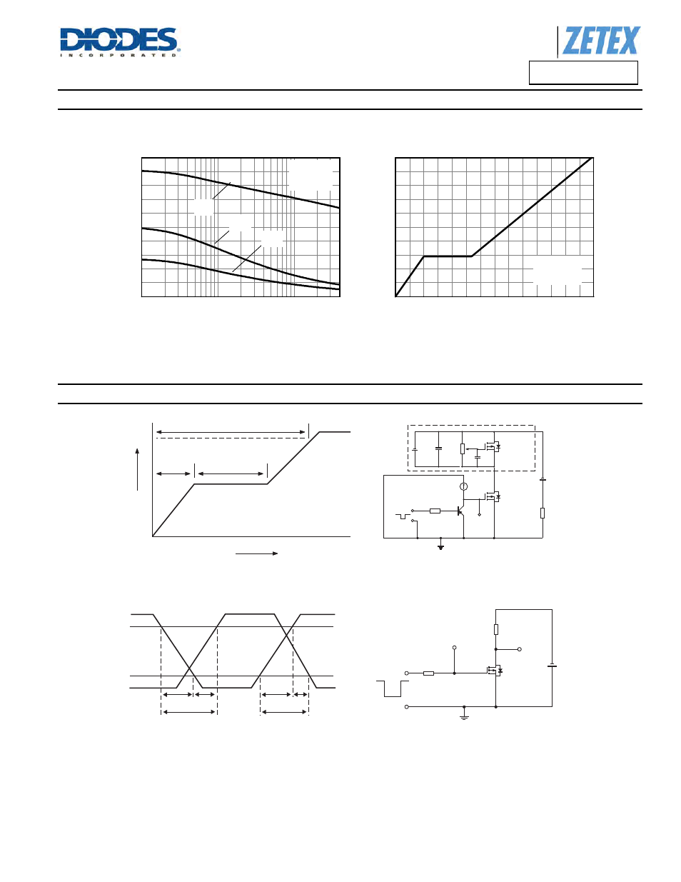
Typical Characteristics –
(cont.)
0.1
1
10
0
200
400
600
800
1000
C
RSS
C
OSS
C
ISS
V
GS
= 0V
f = 1MHz
C
C
a
p
a
c
it
anc
e (
p
F)
-V
DS
- Drain - Source Voltage (V)
0
2
4
6
8
10
12
14
0
2
4
6
8
10
V
DS
= -20V
I
D
= -6A
Gate-Source Voltage v Gate Charge
Capacitance v Drain-Source Voltage
Q - Charge (nC)
-V
GS
G
a
te-S
ource V
o
lt
age (
V
)
Test Circuits
Current
regulator
Charge
Gate charge test circuit
Switching time test circuit
Basic gate charge waveform
Switching time waveforms
D.U.T
50k
0.2
F
12V
Same as
D.U.T
V
GS
V
GS
V
DS
V
G
Q
GS
Q
GD
Q
G
V
GS
90%
10%
t
(on)
t
(on)
t
d(on)
t
r
t
r
t
d(off)
V
DS
V
DD
R
D
R
G
Pulse width
Ͻ 1S
Duty factor 0.1%
V
DS
I
D
I
G
Advertising