Stackup data, Stackup stub, Full stackup – Altera Device-Specific Power Delivery Network User Manual
Page 14
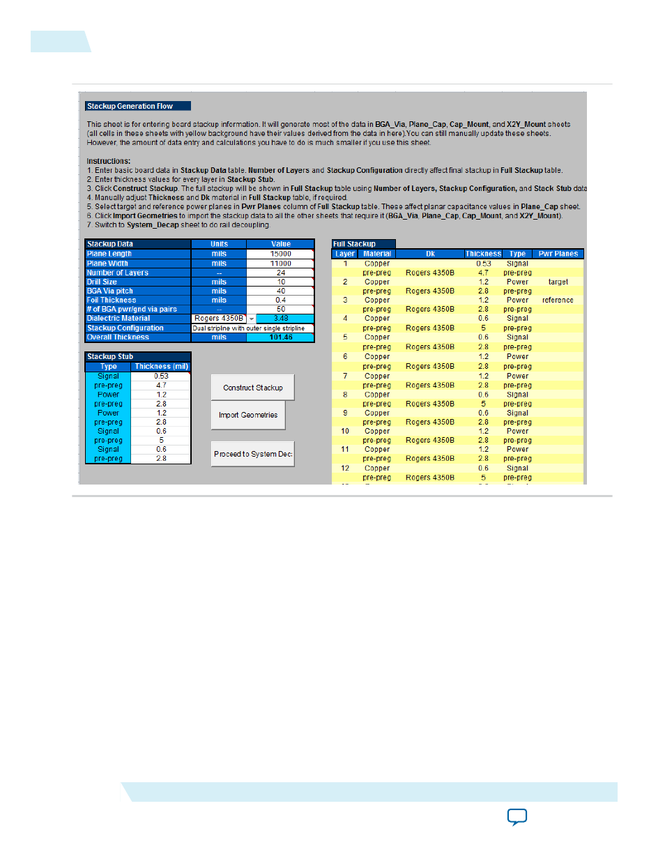
Figure 7: Stackup Tab
Stackup Data
The Stackup Data section is where you enter board dimension data and other parameters, such as board
stackup settings, power via, and dielectric material.
Stackup Stub
The content in this section is updated based on the settings in Stackup Configuration, in the Stackup
Data section. Enter the thickness of the metal/dielectric material for each layer. The stackup shown in this
section is used as the basic unit to construct the complete PCB stackup.
Full Stackup
This section lists the complete stackup of your board. You can modify content in the section to better
match your board design. The last column in the section is the PWR plane types. In a single rail analysis
case, assign the layer where the power rail is located as target, and the ground layer that the power rail
refers to as reference.
14
Stackup Data
UG-01157
2015.03.06
Altera Corporation
Device-Specific Power Delivery Network (PDN) Tool 2.0 User Guide