Timing, Timing components, Timing constraints and files – Altera LVDS SERDES User Manual
Page 19: Figure 10
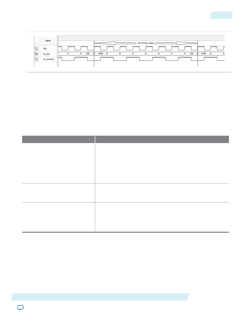
Figure 10: 180° Center Aligned tx_outclock x8 Serializer Waveform with Division Factor of 2
Timing
To properly perform timing analysis on the Altera LVDS SERDES IP core on Arria 10 devices, the Quartus
II software version 14.0a10 generates the required timing constraints.
Timing Components
Table 6: Timing Components
This table lists the timing components for the Altera LVDS SERDES IP core.
Description
Timing Component
The source synchronous paths are paths where clock and data signals
are passed from the transmitting devices to the receiving devices. For
example:
• FPGA/LVDS/TX to external receiving device transmitting path
• External transmitting device to FPGA/non-DPA mode/LVDS/RX
receiving path
Source Synchronous Paths
The I/O capture paths in soft-CDR and DPA-FIFO modes are registered
by a DPA block, which dynamically chooses the best phase from the
PLL VCO clocks to latch the input data.
Dynamic Phase Alignment Paths
The internal FPGA paths are the paths inside the FPGA fabric. This
includes the LVDS RX hardware to core registers paths, core registers
to LVDS TX hardware paths and others core registers to core registers
path. The TimeQuest Timing Analyzer reports the corresponding
timing margins.
Internal FPGA Paths
Timing Constraints and Files
To enable you to perform timing analysis on the Altera LVDS SERDES IP core successfully, the IP core
generates the following timing files, which you can locate in the <variation_name> directory.
Altera Corporation
Altera LVDS SERDES IP Core User Guide
19
Timing
ug_altera_lvds
2014.08.18