Featured device, Featured device -4 – Altera Arria GX Development Board User Manual
Page 14
2–4
Reference Manual
Altera Corporation
Arria GX Development Board
October 2007
Featured Device
Featured Device
The Arria GX Development Kit features the EP1AGX60DF780 FPGA (U7)
in a 780-pin flip-chip FineLine BGA
®
(FBGA) package.
Table 2–2
lists
some Arria GX device features.
Components and Interfaces
J14
PCIe edge connector
A x4 (4 channel) PCI Express edge connector for insertion into
PCI Express-based host platforms.
J13
PCIe mode select jumper
Indicates to the host controlling the Arria GX development
board if the card is operating in either PCIe x1 or PCIe x4
mode.
J2
HSMC interface
High speed mezzanine connector allows for the connection of
HSMC daughter cards.
Power
J1
DC power jack
DC input connector for the board
SW1
Power switch
(1)
Slide switch that enables power to the board.
Note to
Table 2–1
:
(1)
Power switch is bypassed when the board is plugged into a PCI slot.
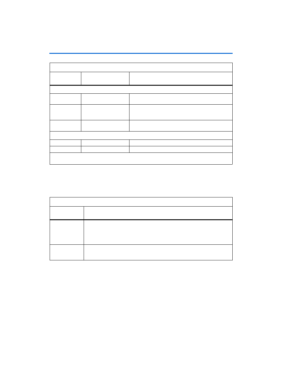
Table 2–1. Board Components & Interfaces (Part 2 of 2)
Board
Reference
Name
Description
Table 2–2. Arria GX Features
Architectural
Feature
Results
The Altera®
low-cost,
protocol-specific,
transceiver-based
FPGA
●
Provides a low-cost, transceiver-based design solution for the most popular high-speed
serial interfaces
●
Provides optimum jitter performance across the entire operating range of 1.25 Gbps to
2.5 Gbps
●
Provides best-in class signal integrity performance
Innovative clock
management
system
●
Clock signals are automatically routed to the appropriate destination
●
Greatly simplifies high-speed board designs