Altera Transceiver Signal Integrity Development Kit, Stratix V GT Edition User Manual
Page 46
2–38
Chapter 2: Board Components
Power Supply
Transceiver Signal Integrity Development Kit
May 2014
Altera Corporation
Stratix V GT Edition Reference Manual
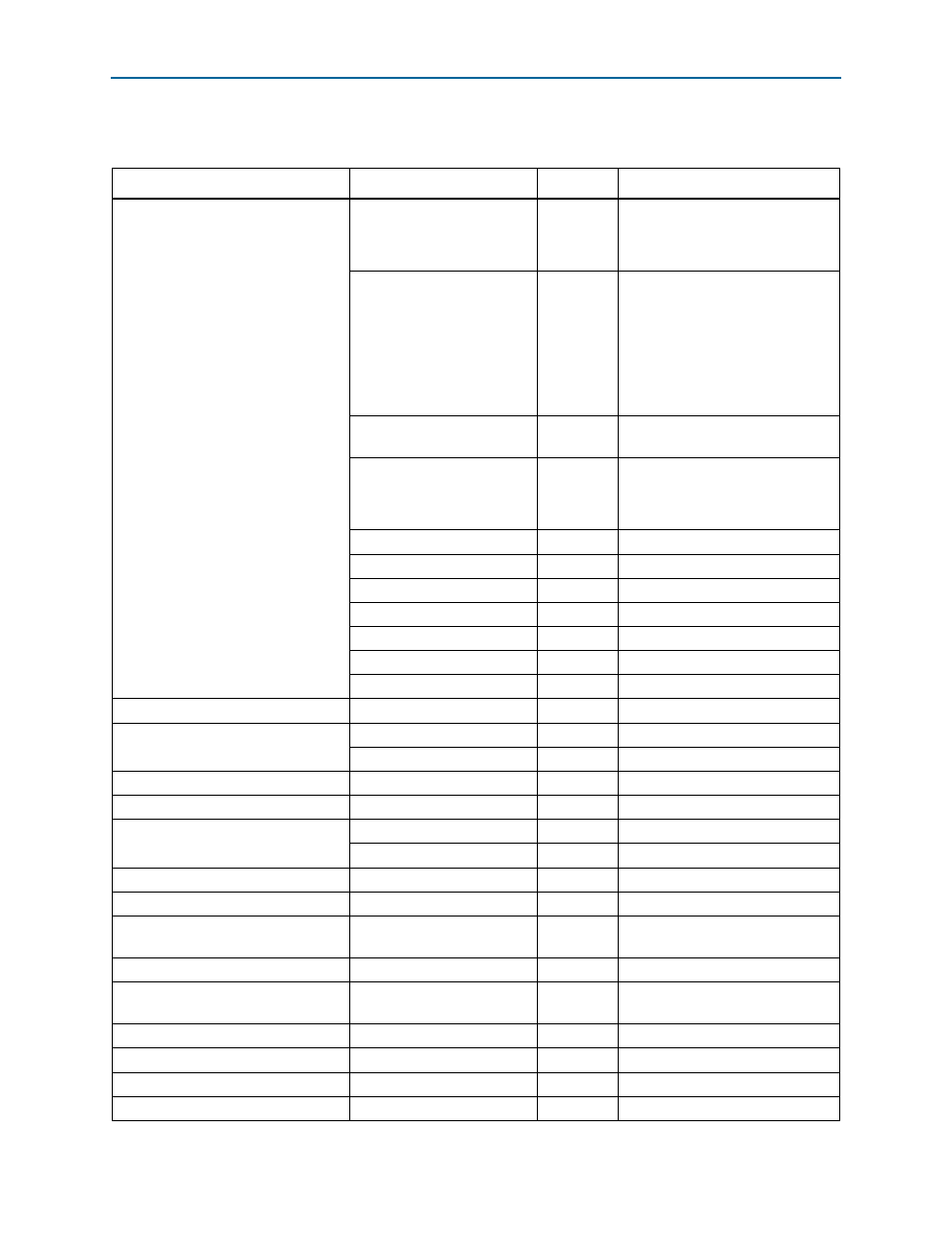
lists the power requirements for each major component on the board.
Table 2–39. Power Requirements
Device
Voltage Name
Voltage (V)
Note
FPGA
S5GX_VCC
0.85
VCC
VCCHIP
VCCHSSI
2p5V
2.5
VCCIO
VCCPD
VCCREF
VCCPGM
VCCBAT
VCC_CLKIN
2p5V_FLTR
2.5
Ferrite fitered from 2p5V,
VCCA_PLL, and VCCAUX
1p5V
1.5
VCCPT
VCCH_GXB
VCCD_FPLL
VCCBAT
1.5
BT1 socket
VCCR_GTB (28G channels)
0.85 or 1.0
LDO
VCCT_GTB (28G channels)
0.85 or 1.0
LDO
VCCL_GTB (28G channels)
0.85 or 1.0
LDO
VCCRT_GXB
0.85 or 1.0
Low noise switcher
VCCA_GXB
2.5 or 3
Low noise switcher
VCCH_GXB
1.5 Tied
to
1p5V
(low noise switcher)
MAX II (for FPP configuration)
2p5V
2.5
—
Flash
2p5V
2.5
Core
XFP_1p8V
1.8
I/O
MAX II (for USB-Blaster)
2p5V
3.3
Core or I/O
EEPROM
USBVCC
5.0
—
USB PHY
USBVCC
5.0
Core
2p5V_USB
2.5
I/O
Power monitor
5V
5.0
—
Temperature sense ADC
3p3V
3.3
—
ICS557-03 spread spectrum clock
buffer (x1)
3p3V
3.3
25-MHz clock output to the FPGA
ICS8304 clock buffer
3p3V/2p5V
3.3/2.5
50-MHz clock outputs
IDT5T9306 transceiver REFCLK clock
buffers (x4)
2p5V
2.5
Programmable clock outputs
T85A23157 dual analog switch
5V
5.0
—
Character LCD
5V
5.0
—
LEDs (x13)
2p5V
2.5
—
Board power LED
5V
5.0
—