Chapter 3: motherboard information, Block diagram, Chapter 3 – Lanner FW-7540 User Manual
Page 15: Motherboard information, Mb-7540 block diagram
10
Motherboard Information
Chapter 3
Network Application Platforms
Chapter 3:
Motherboard Information
Block Diagram
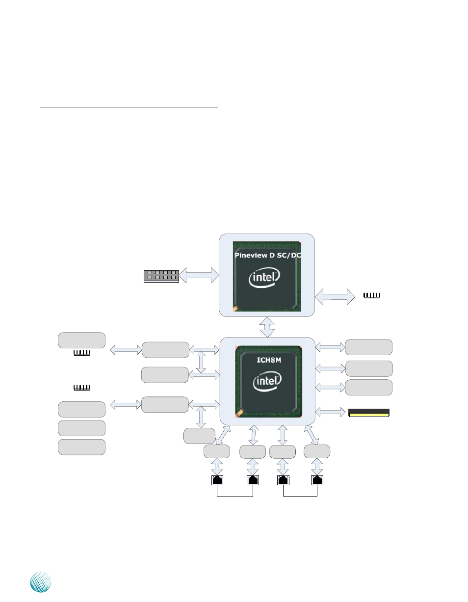
The block diagram depicts the relationships among the
interfaces or modules on the motherboard. Please refer
to the following figure for your motherboard’s layout
design.
MB-7540 Block Diagram
X4 DMI
VG
A
Up to 4GB
MAX
Winbond
W83627
D
HG-
P
LPC
425 / 525
Processor
PC
I-E
x
1
USB
1x DDR3
800Mhz LONG-DIMM
2 x 6 pin Header
SATA
IDE
SPI
PCIE *1 over PCIE * 4
connector
(reserved for future use)
USB
2.0
PC
I-E
x1
USB 2.0
Mini PCI-E
CF II Socket
2 x SATA
SPI ROM
USB 2.0 front
USB pin Header
internal
PCI-E x1
Intel
82583V
PCI-E x1 PCI-E x1 PCI-E x1
Intel
82583V
Intel
82583V
Intel
82583V
1 pair Bypass
1 pair Bypass
Console Port using
RJ-45 connector
Console Pin
Header
KB/Mouse
Voltage Thermal
Sensor
TPM
(optional)
COM1
COM2
LPC Bus
(optional)