Pin assignments, Pin descriptions – Linx Technologies TRM-xxx-DP1203 User Manual
Page 5
– –
– –
4
5
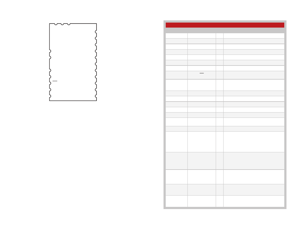
Pin Assignments
Figure 5: DP1203 Series Transceiver Pin Assignments (Top View)
3
2
1
4
5
6
8
7
9
10
11
12
13
14
15
16
17
18
19
20
21
TX
GND
RX
PATTERN
DATAIN
DATA
DCLK
CLKOUT
SCK
SI
SO
GND
VCCP
VCCA
GND
VCC
EN
SWITCH
GND
ANTENNA
GND
Pin Descriptions
Pin
Name
I/O Description
1
GND
Ground
2
ANTENNA
I/O 50-ohm RF Antenna Port
3
GND
—
Ground
4
VCCP
—
Supply Voltage / advised NC
5
VCCA
—
Supply Voltage
6
GND
—
Ground
7
VCC
—
Supply Voltage
8
EN
I
3-wire Interface Communication Enable
Signal.
9
SWITCH
I/O
Selects between two pre-configured states,
e.g. transmit and receive. The states are
determined by the SWParam register.
10
GND
I
Ground
11
GND
I
Ground
12
SO
O
Data output of the 3-wire interface
13
SI
I
Data input of the 3-wire interface
14
SCK
I
Data clock of the 3-wire interface
15
CLKOUT
O
Programmable Clock Output:
F
XTAL
divided by 4, 8, 16 or 32
16
DCLK
O
Receiver Data Clock
17
DATA
I/O
Transmitter Data Input and Receiver
Data Output. This is a bi-directional line
that changes based on the module’s
TX/RX state. This line can be set to the
receiver data output only by disabling the
bidirectional data in the ADParam register.
18
DATAIN
I
Transmitter Data Input. This line is the
transmitter data input when bidirectional
data is disabled using the ADParam register.
This line is not used when bidirectional data
is enabled.
19
PATTERN
O
Output of the Pattern Recognition Block.
This line goes high when the module detects
a received bit pattern that matches a pattern
stored in the Pattern configuration register.
20
RX
I
Antenna Switch RX Select. Set high for
receive mode; must be set opposite the TX
line
21
TX
I
Antenna Switch TX Select. Set high for
transmit mode; must be set opposite the
RX line.
Figure 6: DP1203 Series Transceiver Pin Descriptions
Pin Descriptions