Linx Technologies MDEV-LICAL-HS User Manual
Page 7
–
–
–
–
8
9
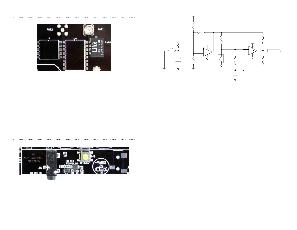
The left side of the circuit consists of an op-amp that is set up as a timer
to feed current into the phototransistor for a specific amount of time after
the button is pressed. Since the phototransistor can pick up infrared
radiation from many sources, including lights, this keeps the output from
randomly switching and keeping the encoder awake. This circuit keeps the
phototransistor from constantly pulling current and allows the encoder to
enter sleep mode, preventing it from also constantly pulling full current.
The circuit works in the following way: when SW8 is pressed, capacitor C4
discharges and pulls the negative input of the op amp low. This makes the
output of the op amp go high and supplies current to the phototransistor
(IR1). C4 begins to recharge through R14 as soon as SW8 is released.
At 5.1M
Ω, it takes approximately 20 seconds for the voltage to get high
enough to make the output of the op amp go low and deactivate IR1.
The right half of the circuit uses a comparator as a data slicer to make
the output of the phototransistor into a square wave that is easier for the
encoder to read. The output of the comparator is then connected to the
KEY_IN line on the encoder. The Master Development board has a 10k
Ω
resistor in series to prevent the jack from shorting the comparator out, but
it may not be necessary in a custom design.
The Encoder Board RF Area
Figure 8 shows the RF area of the development board.
This board can be populated with either the LR Series transmitter (as
shown) or the ES Series transmitter. The LR Series transmitter is placed
on the right side and the ANT1 connector is populated. The ES Series
transmitter is placed on the left and the ANT2 connector is populated.
R27 is connected to the LADJ line of the LR transmitter to reduce the
output power to approximately 0dBm. The LR Series transmitter is capable
of producing more output power than may be legally acceptable, so by
reducing the output power, the range experienced with the evaluation
kit will more closely resemble the range that can be achieved with a final
certified product.
The Encoder Board Key Exchange Area
Figure 9 shows the key exchange area of the development board.
This section allows for both a wire and infrared transfer of the Encryption
Key. The encoder can only receive a key, so only the infrared receiver
and KEY_IN jack are populated. The jack is simply connected directly to
the KEY_IN line on the encoder. The infrared receiver is more complex. A
schematic diagram of this circuit is shown in Figure 10.
Figure 8: The Encoder Board RF Area
Figure 9: The Encoder Board Key Exchange Area
GND
R21
100k
VCC
R18
9.1M
R20
51k
VCC
VCC
GND
GND
GND
C4
4.7uF
R16
9.1M
R15
9.1M
R19
10k
R14
5.1M
R17
9.1M
GND
To KEY_IN
C5
0.01uF
GND
+
-
GND
VCC
+
-
SW8
U6
U6
IR1
Figure 10: The Infrared Receiver Circuit