Master development software, Hs-enc – Linx Technologies MDEV-xxx-HH-CP8-HS User Manual
Page 11
–
–
–
–
16
17
Master Development Software
This software gives a complete understanding of how the HS Series
encoders and decoders work together, as well as showing how they are
used in a system.
The Master Development software can be used in one of two modes.
The default mode is a software simulation of the system and does not
require any hardware. It simulates two handheld transmitters as well as two
receiving devices. This is a good way to illustrate how the HS Series works
in a system by turning on lights and opening doors.
The second mode is for use with the Master Development System. When
the decoder board is plugged into a USB port on the PC, the transmitter
can be used to activate the features in the software. If the LEDs on the
evaluation board turn on, then the LEDs in the program turn on and
activate the corresponding data line function.
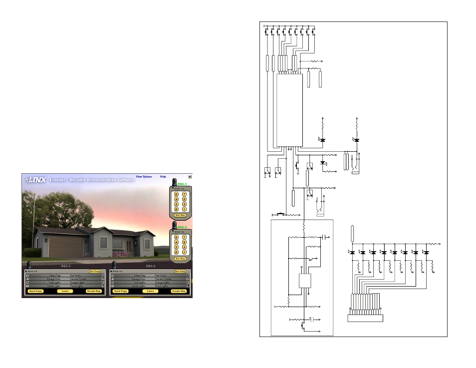
Figure 17 is a screen shot of the program set up in Software Operation
Mode for simulating the operation of the system.
The transmitters are on the right hand side and the receivers are at the
bottom. Complete instructions for using the software can be found by
clicking on the Help label at the top right of the window.
LATCH
RA2/AN2
1
RA3/AN3
2
RA4/AN4
3
RA5/MCLR
4
GND
5
GND
6
RB0/INT
7
RB1
8
RB2/RX
9
RB3
10
RB4
11
RB5/TX
12
RB6/AN5
13
RB7/AN6
14
VCC
15
VCC
16
RA6
17
RA7
18
RA0/AN0
19
RA1/AN1
20
U7
PIC16LF88
GND
VCC
GND
VCC
GND
GND
GND
GND
GND
D7
D4
TX_ID
D6
D3
D0
D1
D2
D5
DATA_PC
PDN
DEC_DATA
GND
GND
VCC
RF1
ES RF
1
GND
2
NC
3
GND
4
VCC
5
LR PDN
6
LR RSSI
7
LR DATA
8
NC
9
ES AUDIO REF 10
ES AUDIO
11
ES DATA
12
ES RSSI
13
ES PDN
14
GND
15
LR RF
16
U4
RXM-XXX-LR
RXM-XXX-ES
GND
PDN
DEC_DATA
RF2
ANT1
REVSMAPCB
GND
RF1
ANT2
REVSMAPCB
GND
RF2
DATA_PC
5V
1
DAT -
2
DAT+
3
GND
4
GSHD
5
GSHD
6
J2
USB-B
USBDP
1
USBDM
2
GND
3
VCC
4
SUSP IND
5
RX IND
6
TX IND
7
485 TX
8
DTR 9
CTS 10
RTS 11
DATA OUT 12
DATA IN 13
DSR 14
DCD 15
RI 16
U5
SDM-USB-QS
GND
GND
GND GND
R9
200
D11
RX_IND
R10
200
D10
TX_ID
D7
D4
D6
DEC_DAT
A
D3
D0 D1 D2
D5
GND
D2
D2_IN
D
D3
D3_IN
D
D4
D4_IN
D
D5
D5_IN
D
D6
D6_IN
D
GND
R1
1
200
D7
D7_IN
D
D0
D0_IN
D
D1
D1_IN
D
SEND
PDN
R7
100K
R6
100K
R0
100K
R1
100K
R2
100K
R3
100K
R4
100K
R5
100K
D
ATA_OUT
TX_ID
GND
GND
GND
GND
GND
GND
GND
GND
1
2
3
4
5
6
7
8
9
10
11
12
13
14
J3
CON1
4
GND
B1
9V BATTERY
GND
SW15
POWER SWITCH
GND
+ C1
220uF
GND
VCC
C2
10uF
GND
VCC
D9
DIODE400
Vb
SW Vb
Va
J1
PWRJACK
GND
GND
1
Vout 2
Vi
n
3
U2
VREG-3V
VREG-5V (ES RX ONLY)
PDN
1
LVL/AM
2
VCC
3
GND
4
DATA
5
/CLK
6
/CLK SEL
7
LV DET
8
GND
9
RF
10
U8
TXM-xxx-ES
GND
VCC
DATA_OUT
PDN
RF2
GND
VCC
GND
1
DATA IN
2
GND
3
LADJ/VCC
4
RF OUT 5
GND
6
VCC
7
PDN
8
U3
TXM-xxx-LR
GND
VCC
GND
GND
DATA_OUT
PDN
RF1
R27
620ohm
ENCODER / DECODER SECTION
POWER SUPPLY SECTION
USB SECTION
RF SECTION
VCC
GND
R1
3
100k
GND
DEC_DAT
A
GND
R2
2
100k
LATCH
SW9 HS_SEND_KEY
VCC
SW1
3
HS_CREATE_KEY
VCC
J5
HS_KEY_IN
J4
HSD_KEY_OUT
GND
GND
R2
5
200
D1
2
MODE_IN
D
GND GND
SW1
6
CREATE/LEARN
GND
R2
3
100K
DATA_OUT
VCC
GND
D7
D4
D6
D3
D0
D1
D2
D5
VCC VCC
S5
D5
VC
C
S4
D4
S3
D3
S2
D2
S1
D1
S0
D0
S6
D6
S7
D7
PDN
SEND
VCC
GND
R1
2
100k
R2
6
0K
D6 D7 SEL_BAUD0 SEL_BAUD1/HSE_SEL_TIMER/HSD_SEND_COPY GND GND HSD_COPY_IN/HSE_KEY_IN/MSE_GND/MSD_LATC
H
TX_CNTL/MSD_RX_CNTL/HSD_CREATE_KEY DATA_OUT/MSD_TX_ID/HSD_KEY_OUT MODE_IN
D
MSE_CREATE_ADDR/HSE_CREATE_PIN/DEC_LEARN
SEND/DEC_DATA_IN
D0
D1
VC
C
VC
C
D2
D3
D4
D5
U1
LICAL-XXX-MS
LICAL-XXX-HS
SW1
1
SEL_BAUD0
TX_ID
SW1
0
LATC
H
SW1
4
PDN
SW1
2
SEL_BAUD1
GND
AOUT
1
AIN-
2
AIN+
3
GND
4
CIN+
5
CIN-
6
COUT
7
VCC
8
U6
TLV2302
HS-ENC
R2
1
100K
VCC
R1
8
9.1M
R2
0
51K
C5 0.01uF
VCC
VCC
GND
GND
GND
GND
C4 4.7uF
R1
6
9.1M
R1
5
9.1M
R1
9
10K
R1
4
5.1M
R1
7
9.1M
IR
1
PS1102
SW8
SW-PB
GND
IR
2
IR
KEY_OUT
R2
4
150 ohm
GND
GND
R8 200
D8
TX_EN
R2
8
10K
Figure 17: HS Encoder / Decoder Demonstration Software
Figure 18: Encoder / Decoder Section Schematic Diagram