Displays, And-tft-5vx-kit – Purdy AND-TFT-5VX-KIT User Manual
Page 5
AND-TFT-5VX-KIT
Displays
Purdy Electronics Corporation • 720 Palomar Avenue • Sunnyvale, CA 94085
05/13/03
Tel: 408.523.8200 • Fax: 408.733.1287 • [email protected] • www.purdyelectronics.com
5
CN 2
Note 1: Gate off voltage, V
EE
=10V.
Note 2 : Gate on voltage, V
GG
=19V.
Note 3 : Select up or down shift (
see Table 1
)
Note 4 : Gate driver shift clock
Note 5 : When OE is connected to high “1”, the driver outposts
are disabled (Gate output=V
EE
). Under this condition,
the operation of registers will not be affected.
Note 6 : Select left or right shift (
see Table 2
)
Note 7 : Latch the polarity of outputs and switch the new data
to outputs. At the rising edge (LD), latch the “POL”
signal to control the polarity of the outputs.
Note 8 : Control whether the Data RO~G5 are inverted or not.
(PVI suggests connecting to GND) When “REV=1”
these data will be inverted. EX: “00”
to “3F”, “07” to
“38”, “15” to “2A”
Note 9 : Polarity selector for dot-inversion control. Available
at the rising edge of LD. When POL=1: Even outputs
range from V1~V7, and Odd outputs range from
V8~V14, and Odd outputs range from V1~V7.
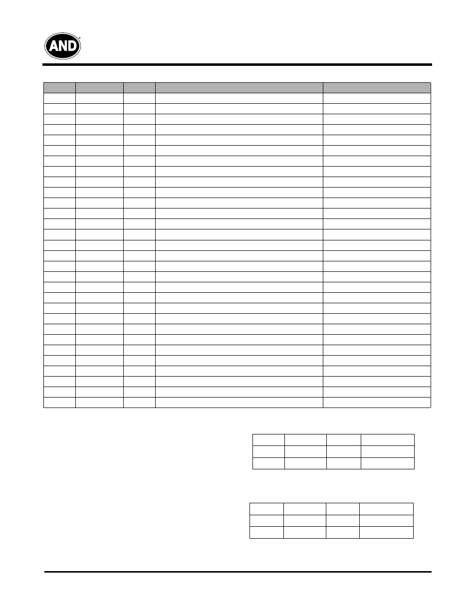
Pin #.
Symbol
I/O
Function
Remark
1
VSS2
|
Ground
2
V1
I
Gamma Voltage 1
3
V2
I
Gamma Voltage 2
4
V3
I
Gamma Voltage 3
5
V4
I
Gamma Voltage 4
6
V5
I
Gamma Voltage 5
7
V6
I
Gamma Voltage 6
8
V7
I
Gamma Voltage 7
9
VSS2
I
Ground
10
V8
I
Gamma Voltage 8
11
V9
I
Gamma Voltage 9
12
V10
I
Gamma Voltage 10
13
V11
I
Gamma Voltage 11
14
V12
I
Gamma Voltage 12
15
V13
I
Gamma Voltage 13
16
V14
I
Gamma Voltage 14
17
VSS2
I
Ground
18
VDD2
I
Voltage for analog circuit
19
VCOM
I
Common Voltage
20
XON
I
NC
21
OE
I
Output Enable
Note 5
22
U/D
I
Right / Left Selection
Note 3
23
CKV
I
Vertical Shift Cllock
Note 4
24
STVU
I
Vertical Shift Pulse Signal Input or Output
Note 3
25
STVD
I
Vertical Shift Pulse Signal Input or Output
Note 3
26
VGG
I
Gate On Voltage
Note 2
27
GND
I
Ground
28
VCC
I
Voltage for logic circuit
29
GND
I
Ground
30
VEE
I
Gate Off Voltage
Note 1
Table 1
U / D
STVU
STVD
Shift
1
Hi-Z
Input
Down to Up
0
Input
Hi-Z
Up to Down
Table 2
R / L
D
|
O2
D|O2
Shift
1
Input
Hi-Z
Left to Right
0
Hi-Z
Input
Right to Left