Input parameter, Input parameter –2 – Altera PowerPlay Early Power Estimator for Altera CPLDs User Manual
Page 12
2–2
Chapter 2: PowerPlay Early Power Estimator Worksheets
Power Estimation Using the PowerPlay Early Power Estimator
PowerPlay Early Power Estimator for Altera CPLDs User Guide
December 2010
Altera Corporation
1
Only use the results obtained as an estimation of power, not as a specification of
power. The actual I
CC
must be verified during device operation, as this measurement
is sensitive to the actual pattern in the device and the environmental operating
conditions.
The accuracy of the power estimation depends on the information you enter. The
power consumed can also vary depending on the toggle rates you enter. The
following sections describe the sections in the Main worksheet of the PowerPlay EPE
spreadsheets.
Input Parameter
Different MAX II and MAX V devices consume different amounts of power for the
same design. The larger the device, the more power it consumes because of a larger
clock tree.
lists the values you must specify in the Input Parameter section in the Main
worksheet of the PowerPlay EPE spreadsheet, as shown in
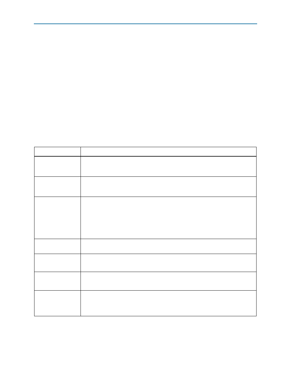
Table 2–1. Input Parameter Section Information
Input Parameter
Description
Device
Select your device.
Larger devices consume more static power and have higher clock dynamic power. All power
components are unaffected by the device you use.
Package
Select the package that you are using.
Larger packages provide a larger cooling surface and more contact points to the circuit board,
leading to lower thermal resistance. Package selection does not affect dynamic power.
Temperature Grade
Select the appropriate temperature grade. This field only affects the allowed maximum junction
temperature range.
Different device families support different temperature grades. For more information about the
supported temperature grade and the recommended operating range for the device junction
temperature, refer to the
apter in the MAX II Device
Handbook and the
hapter in the MAX V
Device Handbook.
Power Characteristics
Select the typical or theoretical worst-case silicon process.
There is a process variation from die-to-die. This primarily impacts static power consumption.
V
CCINT
Supply Voltage
The voltage of the V
CCINT
power supply. For MAX IIG, MAX IIZ, and MAX V devices, the supply
voltage is 1.8 V. For other MAX II devices, it can be either 2.5 V or 3.3 V. Devices with lower
V
CCINT
have lower total standby power consumption.
Ambient Temperature,
T
A
(°C)
Enter the air temperature near the CPLD device. This value can range from –40°C to 125°C,
depending on the device temperature grade. This parameter is used to compute junction
temperature based on power dissipation and thermal resistances through the top of the chip.
Airflow
Select an available ambient airflow in linear-feet per minute (lfm) or meters per second (m/s).
The values are 100 lfm (0.5 m/s), 200 lfm (1.0 m/s), 400 lfm (2.0 m/s), or Still Air.
Increased airflow results in a lower junction-to-air thermal resistance and lowers the junction
temperature.