Serial output specification – MicroE 3500Si Mercury User Manual
Page 18
Page 16
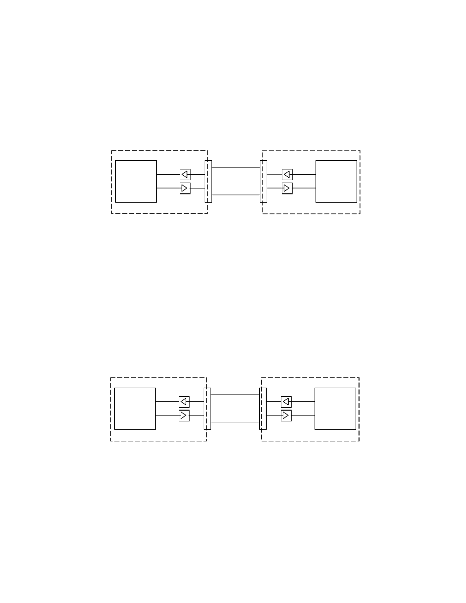
Serial Clock Feedback
The Serial Clock Feedback (SCF) signal may be used to compensate for propagation delays caused by line receivers/drivers and the interface
cabling between the SS350cSi and the customer electronics. The spiClockIn (SCK) signal is "looped" back as an output to create the Serial Clock
Feedback signal. Please see Delay Diagram below:
Note: The timing diagram information lists the timing delays between a request for data at point A and the receipt of data at point B. It does not
include the interface cable, line drivers/receivers or any other electronics needed at the customer interface for signal acquisition.
Maximum Propagation Delay. (Serial Clock Feedback - not used)
FPGA
40 nsec
receiver 35 nsec
driver 10 nsec
MicroE SS-350cSi
A
B
Interface
Cable
Customer’s
electronics
Customer’s interface timing
d1
d7
d2
d3
d4
d5
d6
There is a propagation delay due to the clock being sampled at position A and the Data being sampled at position B.
Propagation Delay = d1+d2+d3+d4+d5+d6+d7
Maximum Propagation Delay. (Serial Clock Feedback signal implemented)
Propagation delay is eliminated because both data and clock are sampled at position B
System Latency=d1+d2+d3+d4+d5+d6+d7
FPGA
40 nsec
receiver 35 nsec
driver 10 nsec
MicroE SS-350cSi
A
B
Interface
Cable
Customer’s
electronics
Customer’s interface timing
d1
d7
d2
d3
d4
d5
d6